PSD853F2-90J STMicroelectronics, PSD853F2-90J Datasheet - Page 33

PSD853F2-90J
Manufacturer Part Number
PSD853F2-90J
Description
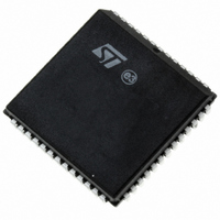
IC FLASH 1MBIT 90NS 52PLCC
Manufacturer
STMicroelectronics
Datasheet
1.PSD813F2VA-20JI.pdf
(109 pages)
Specifications of PSD853F2-90J
Format - Memory
FLASH
Memory Type
FLASH
Memory Size
1M (128K x 8)
Speed
90ns
Interface
Parallel
Voltage - Supply
4.5 V ~ 5.5 V
Operating Temperature
0°C ~ 70°C
Package / Case
52-PLCC
Lead Free Status / RoHS Status
Contains lead / RoHS non-compliant
Other names
497-2021-5
Available stocks
Company
Part Number
Manufacturer
Quantity
Price
Company:
Part Number:
PSD853F2-90J
Manufacturer:
STMicroelectronics
Quantity:
10 000
Company:
Part Number:
PSD853F2-90JI
Manufacturer:
STMicroelectronics
Quantity:
10 000
Part Number:
PSD853F2-90JI
Manufacturer:
WSI
Quantity:
20 000
PLDS
The PLDs bring programmable logic functionality
to the PSD. After specifying the logic for the PLDs
using the PSDabel tool in PSDsoft Express, the
logic is programmed into the device and available
upon Power-up.
The PSD contains two PLDs: the Decode PLD
(DPLD), and the Complex PLD (CPLD). The PLDs
are briefly discussed in the next few paragraphs,
and in more detail in the section entitled
PLD (DPLD), page 35
Complex
13., page 34
The DPLD performs address decoding for Select
signals for internal components, such as memory,
registers, and I/O ports.
The CPLD can be used for logic functions, such as
loadable counters and shift registers, state ma-
chines, and encoding and decoding logic. These
logic functions can be constructed using the 16
Output Macrocells (OMC), 24 Input Macrocells
(IMC), and the AND Array. The CPLD can also be
used to generate External Chip Select (ECS0-
ECS2) signals.
The AND Array is used to form product terms.
These product terms are specified using PSDabel.
An Input Bus consisting of 73 signals is connected
to the PLDs. The signals are shown in Table 14.
The Turbo Bit in PSD
The PLDs in the PSD can minimize power con-
sumption by switching off when inputs remain un-
changed for an extended time of about 70ns.
Resetting the Turbo Bit to '0' (Bit 3 of PMMR0) au-
tomatically places the PLDs into standby if no in-
puts are changing. Turning the Turbo mode off
increases propagation delays while reducing pow-
er consumption. See the section entitled
MANAGEMENT, page 62
Bit.
PLD
shows the configuration of the PLDs.
(CPLD), page
and the section entitled
on how to set the Turbo
36.
Doc ID 10552 Rev 3
POWER
Decode
Figure
Note: 1. The address inputs are A19-A4 in 80C51XA mode.
Additionally, five bits are available in PMMR2 to
block MCU control signals from entering the PLDs.
This reduces power consumption and can be used
only when these MCU control signals are not used
in PLD logic equations.
Each of the two PLDs has unique characteristics
suited for its applications. They are described in
the following sections.
Table 14. DPLD and CPLD Inputs
MCU Address Bus
MCU Control Signals
Reset
Power-down
Port A Input
Macrocells
Port B Input
Macrocells
Port C Input
Macrocells
Port D Inputs
Page Register
Macrocell AB
Feedback
Macrocell BC
Feedback
Secondary Flash
memory Program
Status Bit
Input Source
1
PSD813F2V, PSD854F2V
MCELLAB.FB7-
MCELLBC.FB7-
CNTL2-CNTL0
PGR7-PGR0
Input Name
Ready/Busy
PC7-PC0
PD2-PD0
PB7-PB0
PA7-PA0
A15-A0
PDN
RST
FB0
FB0
Number
Signals
33/109
16
of
3
1
1
8
8
8
3
8
8
8
1


