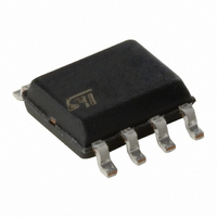
M93S46-MN6T STMicroelectronics, M93S46-MN6T Datasheet - Page 5

M93S46-MN6T
Manufacturer Part Number
M93S46-MN6T
Description
IC EEPROM 1KBIT 1MHZ 8SOIC
Manufacturer
STMicroelectronics
Datasheet
1.M93S46-WMN6TP.pdf
(34 pages)
Specifications of M93S46-MN6T
Format - Memory
EEPROMs - Serial
Memory Type
EEPROM
Memory Size
1K (64 x 16)
Speed
1MHz
Interface
Microwire, 3-Wire Serial
Voltage - Supply
4.5 V ~ 5.5 V
Operating Temperature
-40°C ~ 85°C
Package / Case
8-SOIC (3.9mm Width)
Lead Free Status / RoHS Status
Contains lead / RoHS non-compliant
Other names
497-1938-2
Available stocks
Company
Part Number
Manufacturer
Quantity
Price
Company:
Part Number:
M93S46-MN6T
Manufacturer:
INTERSIL
Quantity:
132
Part Number:
M93S46-MN6T
Manufacturer:
ST
Quantity:
20 000
An internal Power-on Data Protection mechanism
in the M93Sx6 inhibits the device when the supply
is too low.
POWER-ON DATA PROTECTION
To prevent data corruption and inadvertent write
operations during power-up, a Power-On Reset
(POR) circuit resets all internal programming cir-
cuitry, and sets the device in the Write Disable
mode.
–
–
For the M93Sx6 devices (5V range) the POR
threshold voltage is around 3V. For the M93Sx6-
W (3V range) and M93Sx6-R (2V range) the POR
threshold voltage is around 1.5V.
At Power-up and Power-down, the device
must not be selected (that is, Chip Select Input
(S) must be driven Low) until the supply
voltage reaches the operating value V
specified in
When V
properly reset (in the Write Disable mode) and
is ready to decode and execute incoming
instructions.
CC
reaches its valid level, the device is
Table 5.
to
Table
6..
CC
INSTRUCTIONS
The instruction set of the M93Sx6 devices con-
tains seven instructions, as summarized in
2.
lowing parts, as shown in
The M93Sx6 devices are fabricated in CMOS
technology and are therefore able to run as slow
as 0 Hz (static input signals) or as fast as the max-
imum ratings specified in
to
Each instruction is preceded by a rising edge
on Chip Select Input (S) with Serial Clock (C)
being held Low.
A start bit, which is the first ‘1’ read on Serial
Data Input (D) during the rising edge of Serial
Clock (C).
Two op-code bits, read on Serial Data Input
(D) during the rising edge of Serial Clock (C).
(Some instructions also use the first two bits of
the address to define the op-code).
The address bits of the byte or word that is to
be accessed. For the M93S46, the address is
made up of 6 bits (see
M93S56 and M93S66, the address is made up
of 8 bits (see
Table
3.. Each instruction consists of the fol-
Table
M93S66, M93S56, M93S46
3.).
Table 16.
Figure
Table
4.:
2.). For the
to
Table
Table
19..
5/34


