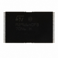
M29W640FB70N6E NUMONYX, M29W640FB70N6E Datasheet - Page 25

M29W640FB70N6E
Manufacturer Part Number
M29W640FB70N6E
Description
IC FLASH 64MBIT 70NS 48TSOP
Manufacturer
NUMONYX
Series
Axcell™r
Datasheet
1.M29W640FB70ZA6E.pdf
(71 pages)
Specifications of M29W640FB70N6E
Format - Memory
FLASH
Memory Type
FLASH - Nor
Memory Size
64M (8Mx8, 4Mx16)
Speed
70ns
Interface
Parallel
Voltage - Supply
2.7 V ~ 3.6 V
Operating Temperature
-40°C ~ 85°C
Package / Case
48-TSOP
Supply Voltage Range
2.7V To 3.6V
Memory Case Style
TSOP
No. Of Pins
48
Access Time
70ns
Base Number
29
Ic Generic Number
29W640
Memory Configuration
8M X 8, 4M X 16
Interface Type
CFI, Parallel
Rohs Compliant
Yes
Lead Free Status / RoHS Status
Lead free / RoHS Compliant
Other names
497-5031
497-5031
497-5031
Available stocks
Company
Part Number
Manufacturer
Quantity
Price
Part Number:
M29W640FB70N6E
Manufacturer:
NUMONYX
Quantity:
20 000
4.2.5
4.2.6
4.2.7
Quadruple Word Program command
This is used to write a page of four adjacent Words (or 8 adjacent Bytes), in x16 mode,
simultaneously. The addresses of the four Words must differ only in A1 and A0.
Five bus write cycles are necessary to issue the command:
To perform the Quadruple Byte Program command, it is necessary to apply V
V
Unlock Bypass command
The Unlock Bypass command is used in conjunction with the Unlock Bypass Program
command to program the memory faster than with the standard program commands. When
the cycle time to the device is long, considerable time saving can be made by using these
commands. Three Bus Write operations are required to issue the Unlock Bypass command.
Once the Unlock Bypass command has been issued the memory will only accept the Unlock
Bypass Program command and the Unlock Bypass Reset command. The memory can be
read as if in Read mode.
When V
Unlock Bypass mode and the Unlock Bypass Program command can be issued
immediately.
Unlock Bypass Program command
The Unlock Bypass command is used in conjunction with the Unlock Bypass Program
command to program the memory. When the cycle time to the device is long, considerable
time saving can be made by using these commands. Three Bus Write operations are
required to issue the Unlock Bypass command.
Once the Unlock Bypass command has been issued the memory will only accept the Unlock
Bypass Program command and the Unlock Bypass Reset command. The memory can be
read as if in Read mode.
The memory offers accelerated program operations through the V
When the system asserts V
enters the Unlock Bypass mode. The system may then write the two-cycle Unlock Bypass
program command sequence. The memory uses the higher voltage on the V
Protect pin, to accelerate the Unlock Bypass Program operation.
Never raise V
memory may be left in an indeterminate state.
PP
/WP pin.
The first bus cycle sets up the command.
The second bus cycle latches the Address and the Data of the first Word to be written.
The third bus cycle latches the Address and the Data of the second Word to be written.
The fourth bus cycle latches the Address and the Data of the third Word to be written.
The fifth bus cycle latches the Address and the Data of the fourth Word to be written
and starts the Program/Erase Controller.
PP
is applied to the V
PP
/Write Protect to V
PP
PP
on the V
/Write Protect pin the memory automatically enters the
PP
from any mode except Read mode, otherwise the
PP
/Write Protect pin, the memory automatically
PP
/Write Protect pin.
PP
PPH
/Write
to the
25/71


