M25P128-VMF6P NUMONYX, M25P128-VMF6P Datasheet - Page 26
M25P128-VMF6P
Manufacturer Part Number
M25P128-VMF6P
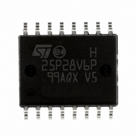
Description
IC FLASH 128MBIT 50MHZ 16SOIC
Manufacturer
NUMONYX
Series
Forté™r
Datasheet
1.M25P128-VME6TGB.pdf
(47 pages)
Specifications of M25P128-VMF6P
Format - Memory
FLASH
Memory Type
FLASH
Memory Size
128M (16M x 8)
Speed
50MHz
Interface
SPI, 3-Wire Serial
Voltage - Supply
2.7 V ~ 3.6 V
Operating Temperature
-40°C ~ 85°C
Package / Case
16-SOIC
Cell Type
NOR
Density
128Mb
Access Time (max)
8ns
Interface Type
Serial (SPI)
Boot Type
Not Required
Address Bus
1b
Operating Supply Voltage (typ)
3.3V
Operating Temp Range
-40C to 85C
Package Type
SO W
Sync/async
Synchronous
Operating Temperature Classification
Industrial
Operating Supply Voltage (min)
2.7V
Operating Supply Voltage (max)
3.6V
Word Size
8b
Number Of Words
16M
Supply Current
8mA
Mounting
Surface Mount
Pin Count
16
Lead Free Status / RoHS Status
Lead free / RoHS Compliant
Other names
Q2855929
Q3097367
Q3097367
Available stocks
Company
Part Number
Manufacturer
Quantity
Price

Part Number:
M25P128-VMF6P
Manufacturer:
ST
Quantity:
20 000
Company:
Part Number:
M25P128-VMF6PB
Manufacturer:
CIRRUS
Quantity:
320
Part Number:
M25P128-VMF6PB
Manufacturer:
ST
Quantity:
20 000
Company:
Part Number:
M25P128-VMF6PB,M25P128-VMF6TP
Quantity:
70


6.6
26/47
Read data bytes (READ)
The device is first selected by driving Chip Select (S) Low. The instruction code for the Read
Data Bytes (READ) instruction is followed by a 3-byte address (A23-A0), each bit being
latched-in during the rising edge of Serial Clock (C). Then the memory contents, at that
address, is shifted out on Serial Data Output (Q), each bit being shifted out, at a maximum
frequency f
The instruction sequence is shown in
The first byte addressed can be at any location. The address is automatically incremented
to the next higher address after each byte of data is shifted out. The whole memory can,
therefore, be read with a single Read Data Bytes (READ) instruction. When the highest
address is reached, the address counter rolls over to 000000h, allowing the read sequence
to be continued indefinitely.
The Read Data Bytes (READ) instruction is terminated by driving Chip Select (S) High. Chip
Select (S) can be driven High at any time during data output. Any Read Data Bytes (READ)
instruction, while an Erase, Program or Write cycle is in progress, is rejected without having
any effects on the cycle that is in progress.
Figure 13. Read data bytes (READ) instruction sequence and data-out sequence
S
C
D
Q
R
0
, during the falling edge of Serial Clock (C).
1
High Impedance
2
Instruction
3
4
5
6
7
MSB
23
8
22 21
9 10
Figure
24-Bit Address
13.
3
28 29 30 31 32 33 34 35
2
1
0
MSB
7
6
5
Data Out 1
4
3
36 37 38
2
1
0
39
7
Data Out 2
AI03748D
Related parts for M25P128-VMF6P
Image
Part Number
Description
Manufacturer
Datasheet
Request
R

Part Number:
Description:
IC FLASH 128MBIT 50MHZ 16SOIC
Manufacturer:
NUMONYX
Datasheet:

Part Number:
Description:
IC FLASH 128MBIT 65NM 3V 8VDFPN
Manufacturer:
NUMONYX
Datasheet:
Part Number:
Description:
IC FLASH 128MBIT 65NM 3V SO16
Manufacturer:
NUMONYX
Datasheet:
Part Number:
Description:
FLASH SERL-SPI 3.3V 128MBIT 16MX8 8NS 16SOIC W
Manufacturer:
NUMONYX
Part Number:
Description:
FLASH SERL-SPI 3.3V 128MBIT 16MX8 8NS 8PIN VDFPN
Manufacturer:
NUMONYX
Part Number:
Description:
IC FLASH 128MBIT 50MHZ 8VDFPN
Manufacturer:
NUMONYX
Datasheet:

Part Number:
Description:
IC FLASH 128MBIT 50MHZ 8VDFPN
Manufacturer:
NUMONYX
Datasheet:

Part Number:
Description:
128 Mbit (Multilevel), low-voltage, Serial Flash memory with 50-MHz SPI bus interface
Manufacturer:
Numonyx, B.V.
Datasheet:
Part Number:
Description:
128 Mbit (Multilevel), low-voltage, Serial Flash memory with 50-MHz SPI bus interface
Manufacturer:
Numonyx, B.V.
Datasheet:
Part Number:
Description:
Numonyx� Embedded Flash Memory J3 V. D
Manufacturer:
Numonyx
Datasheet: