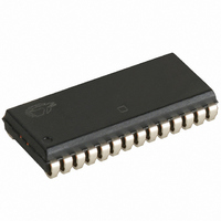
CY7C1399B-15VXI Cypress Semiconductor Corp, CY7C1399B-15VXI Datasheet

CY7C1399B-15VXI
Specifications of CY7C1399B-15VXI
Related parts for CY7C1399B-15VXI
CY7C1399B-15VXI Summary of contents
Page 1
... The input/output pins remain in a high-impedance state unless the chip is selected, outputs are enabled, and Write Enable (WE) is HIGH. The CY7C1399B is available in 28-pin standard 300-mil-wide SOJ and TSOP Type I packages. POWER DOWN ...
Page 2
... I CC Output Disabled V = Max GND CC OUT V = Max mA, CC OUT 1/t MAX ≥ V Max ≥ V ≤ MAX , CE ≥ V Max. V – 0.3V [4] ≤ 0.3V, V – 0.3V ≥V – 0. ≤0.3V MAX CY7C1399B I GND Ambient Temperature ° ° 3.3V ±300 +70 C ° ...
Page 3
... CC IN [4] ≥ V ≤ 0.3V, – 0.3V WE≥V –0.3V or WE≤ 0.3V, CC f=f MAX Description Test Conditions T = 25° MHz 351Ω 1.73V CY7C1399B 1399B-15 1399B-20 Min. Max. Min. Max. 2.4 2.4 0.4 0.4 2 +0.3V +0.3V –0.3 0.8 –0.3 0.8 – ...
Page 4
... The minimum write cycle time for write cycle #3 (WE controlled, OE LOW) is the sum of t Document #: 38-05071 Rev. *D [6] Description [7] [7, 8] [7] [7, 8] [9] [7] is less than less than t HZCE LZCE HZOE = Test Loads. Transition is measured ±500 mV from steady state voltage. CY7C1399B 1399B-10 1399B-12 Min. Max. Min. Max ...
Page 5
... CDR Retention Time t Operation Recovery Time R Document #: 38-05071 Rev. *D [6] (continued) Description [7] [7, 8] [7] [7, 8] [9] [7] (Over the Operating Range - L version only) Description Conditions Com’ 2.0V > V – 0.3V > V – 0. < 0.3V IN CY7C1399B 1399B-15 1399B-20 Min. Max. Min. Max ...
Page 6
... Device is continuously selected HIGH for read cycle. 13. Address valid prior to or coincident with CE transition LOW. Document #: 38-05071 Rev. *D DATA RETENTION MODE > CDR OHA ACE t DOE t LZOE 50 CY7C1399B 3. DATA VALID t HZOE t HZCE IMPEDANCE DATA VALID t PD 50% HIGH ICC ISB Page ...
Page 7
... If CE goes HIGH simultaneously with WE HIGH, the output remains in a high-impedance state. 16. During this period, the I/Os are in the output state and input signals should not be applied. Document #: 38-05071 Rev. *D [9, 14, 15 PWE t SD DATA IN [9, 14, 15 DATA [10, 15 DATA t HZWE CY7C1399B VALID SCE VALID VALID IN t LZWE Page ...
Page 8
... Ordering Code 12 CY7C1399B-12VC CY7C1399B-12VXC CY7C1399B-12ZC CY7C1399B-12ZXC CY7C1399BL-12ZC CY7C1399BL-12ZXC CY7C1399B-12VXI 15 CY7C1399B-15VC CY7C1399B-15VXC CY7C1399B-15ZC CY7C1399B-15ZXC CY7C1399BL-15VC CY7C1399BL-15VXC CY7C1399BL-15ZXC CY7C1399B-15VI CY7C1399B-15VXI CY7C1399B-15ZI CY7C1399B-15ZXI 20 CY7C1399B-20ZC CY7C1399B-20ZXC Document #: 38-05071 Rev. *D Mode Deselect/Power-Down Read Write Deselect, Output Disabled Package Name Package Type V21 28-Lead Molded SOJ V21 ...
Page 9
... Cypress against all charges. 28-Lead (300-Mil) Molded SOJ V21 MIN. MAX. PIN 0.291 0.330 0.300 0.350 28 SEATING PLANE 0.120 0.140 0.004 0.025 MIN. CY7C1399B A DETAIL EXTERNAL LEAD DESIGN 0.026 0.032 0.013 0.014 0.019 0.020 OPTION 1 OPTION 2 0.007 0.013 0.262 0.272 ...
Page 10
... Document History Page Document Title: CY7C1399B 256K(32K x 8) Static RAM Document Number: 38-05071 ISSUE REV. ECN NO. DATE ** 107264 05/25/01 *A 107533 06/28/01 *B 116472 09/17/02 *C 224340 See ECN *D 386100 See ECN Document #: 38-05071 Rev. *D ORIG. OF CHANGE DESCRIPTION OF CHANGE SZV Change from Spec #: 38-01102 to 38-05071 ...


