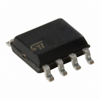
M95640-MN6P STMicroelectronics, M95640-MN6P Datasheet - Page 24

M95640-MN6P
Manufacturer Part Number
M95640-MN6P
Description
IC EEPROM 64KBIT 10MHZ 8SOIC
Manufacturer
STMicroelectronics
Datasheet
1.M95640-WDW6TP.pdf
(48 pages)
Specifications of M95640-MN6P
Format - Memory
EEPROMs - Serial
Memory Type
EEPROM
Memory Size
64K (8K x 8)
Speed
10MHz
Interface
SPI, 3-Wire Serial
Voltage - Supply
4.5 V ~ 5.5 V
Operating Temperature
-40°C ~ 85°C
Package / Case
8-SOIC (3.9mm Width)
Lead Free Status / RoHS Status
Lead free / RoHS Compliant
Available stocks
Company
Part Number
Manufacturer
Quantity
Price
Instructions
6.7
24/48
Figure 13. Page Write (WRITE) sequence
1. Depending on the memory size, as shown in
ECC (error correction code) and Write cycling
The M95640-x and M95640-Dx devices identified with the process letter K offer an ECC
(error correction code) logic which compares each 4-byte word with its associated 6
EEPROM bits of ECC. As a result, if a single bit out of 4 bytes of data happens to be
erroneous during a Read operation, the ECC detects it and replaces it with the correct
value. The read reliability is therefore much improved by the use of this feature.
Note however that even if a single byte has to be written, 4 bytes are internally modified
(plus the ECC bits), that is, the addressed byte is cycled together with the three other bytes
making up the word. It is therefore recommended to write data by word (4 Bytes) at address
4*N (where N is an integer) in order to benefit from the larger amount of Write cycles.
The M95640-x and M95640-Dx devices are qualified at 1 million (1 000 000) Write cycles,
using a cycling routine that writes to the device in multiples of 4-byte words.
Read Identification Page
The Identification Page (32 bytes) is an additional page which can be written and (later)
permanently locked in Read-only mode.
Reading this page is achieved with the Read Identification Page instruction (see
The Chip Select signal (S) is first driven low, the bits of the instruction byte and address
bytes are then shifted in, on Serial Data input (D). Address bit A10 must be 0, address bits
[A15:A11] and [A9:A5] are Don't Care, and the data byte pointed to by [A4:A0] is shifted out
on Serial Data output (Q).
S
C
D
S
C
D
7
32
0
6
33
1
5
34
Data Byte 2
2
4
Instruction
35 36 37 38 39 40 41 42
3
3
4
2
5
Doc ID 16877 Rev 15
1
6
0
7
7
15
8
6
Table
14 13
9 10
5
Data Byte 3
16-Bit Address
7, the most significant address bits are Don’t Care.
4
43
M95640, M95640-W, M95640-R, M95640-DR
3
44 45 46 47
3
20 21 22 23 24 25 26 27
2
2
1
1
0
0
7
6
6
5
Data Byte N
5
Data Byte 1
4
4
3
3
28 29 30
2
2
1
1
0
Table
0
31
AI01796D
4).


