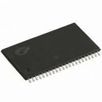
CY14B104N-ZS20XCT Cypress Semiconductor Corp, CY14B104N-ZS20XCT Datasheet - Page 9

CY14B104N-ZS20XCT
Manufacturer Part Number
CY14B104N-ZS20XCT
Description
IC NVSRAM 4MBIT 20NS 44TSOP
Manufacturer
Cypress Semiconductor Corp
Type
NVSRAMr
Datasheet
1.CY14B104N-BA45XC.pdf
(25 pages)
Specifications of CY14B104N-ZS20XCT
Format - Memory
RAM
Memory Type
NVSRAM (Non-Volatile SRAM)
Memory Size
4M (256K x 16)
Speed
20ns
Interface
Parallel
Voltage - Supply
2.7 V ~ 3.6 V
Operating Temperature
0°C ~ 70°C
Package / Case
44-TSOP II
Word Size
16b
Density
4Mb
Interface Type
Parallel
Operating Supply Voltage (typ)
3.3V
Operating Temperature Classification
Commercial
Operating Supply Voltage (max)
3.6V
Operating Supply Voltage (min)
2.7V
Operating Temp Range
0C to 70C
Pin Count
44
Mounting
Surface Mount
Supply Current
65mA
Lead Free Status / RoHS Status
Lead free / RoHS Compliant
AC Switching Characteristics
Switching Waveforms
Notes
Document #: 001-07102 Rev. *L
SRAM Read Cycle
t
t
t
t
t
t
t
t
t
t
t
t
t
t
SRAM Write Cycle
t
t
t
t
t
t
t
t
t
t
t
14. WE must be HIGH during SRAM read cycles.
15. Device is continuously selected with CE, OE and BHE / BLE LOW.
16. Measured ±200 mV from steady state output voltage.
17. If WE is LOW when CE goes LOW, the outputs remain in the high impedance state.
18. HSB must remain HIGH during READ and WRITE cycles.
ACE
RC
AA
DOE
OHA
LZCE
HZCE
LZOE
HZOE
PU
PD
DBE
LZBE
HZBE
WC
PWE
SCE
SD
HD
AW
SA
HA
HZWE
LZWE
BW
Parameters
Cypress
[15]
[13]
[13]
[14]
[15]
[16]
[16]
[16]
[16]
[16]
[16,17]
Parameters
t
t
t
t
t
t
t
t
t
t
t
-
-
-
t
t
t
t
t
t
t
t
t
t
-
ACS
RC
AA
OE
OH
LZ
HZ
OLZ
OHZ
PA
PS
WC
WP
CW
DW
DH
AW
AS
WR
WZ
OW
Parameters
Alt
Chip Enable Access Time
Read Cycle Time
Address Access Time
Output Enable to Data Valid
Output Hold After Address Change
Chip Enable to Output Active
Chip Disable to Output Inactive
Output Enable to Output Active
Output Disable to Output Inactive
Chip Enable to Power Active
Chip Disable to Power Standby
Byte Enable to Data Valid
Byte Enable to Output Active
Byte Disable to Output Inactive
Write Cycle Time
Write Pulse Width
Chip Enable To End of Write
Data Setup to End of Write
Data Hold After End of Write
Address Setup to End of Write
Address Setup to Start of Write
Address Hold After End of Write
Write Enable to Output Disable
Output Active after End of Write
Byte Enable to End of Write
Figure 6. SRAM Read Cycle #1: Address Controlled
Description
Min
20
20
15
15
15
15
3
3
0
0
0
8
0
0
0
3
20 ns
Max
20
20
10
20
10
8
8
8
8
Min
25
25
20
20
10
20
20
3
3
0
0
0
0
0
0
3
[14, 15, 18]
CY14B104L, CY14B104N
25 ns
Max
25
25
12
10
10
25
12
10
10
Min
45
45
30
30
15
30
30
3
3
0
0
0
0
0
0
3
45 ns
Max
45
45
20
15
15
45
20
15
15
Page 9 of 25
Unit
ns
ns
ns
ns
ns
ns
ns
ns
ns
ns
ns
ns
ns
ns
ns
ns
ns
ns
ns
ns
ns
ns
ns
ns
ns
[+] Feedback


