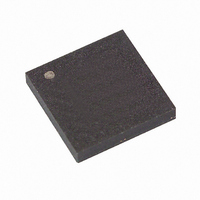
AT17LV65-10CI Atmel, AT17LV65-10CI Datasheet - Page 7

AT17LV65-10CI
Manufacturer Part Number
AT17LV65-10CI
Description
IC SRL CONFIG EEPROM 64K 8-LAP
Manufacturer
Atmel
Datasheet
1.AT17LV65-10CC.pdf
(26 pages)
Specifications of AT17LV65-10CI
Programmable Type
Serial EEPROM
Memory Size
64kb
Voltage - Supply
3 V ~ 3.6 V, 4.5 V ~ 5.5 V
Operating Temperature
-40°C ~ 85°C
Package / Case
8-LAP
For Use With
ATDH2225 - CABLE ISP FOR AT17ATDH2200E - CONFIGURATOR PROGRAM BOARD KIT
Lead Free Status / RoHS Status
Contains lead / RoHS non-compliant
4.1
4.2
4.3
4.4
4.5
4.6
4.7
4.8
4.9
2321I–CNFG–2/08
DATA
CLK
WP1
RESET/OE
WP
WP2
CE
GND
CEO
Three-state DATA output for configuration. Open-collector bi-directional pin for programming.
Clock input. Used to increment the internal address and bit counter for reading and
programming.
WRITE PROTECT (1). Used to protect portions of memory during programming. Disabled
by default due to internal pull-down resistor. This input pin is not used during FPGA loading
operations. This pin is only available on AT17LV512/010/002 devices.
Output Enable (active High) and RESET (active Low) when SER_EN is High. A Low level on
RESET/OE resets both the address and bit counters. A High level (with CE Low) enables the
data output driver. The logic polarity of this input is programmable as either RESET/OE or
RESET/OE. For most applications, RESET should be programmed active Low. This document
describes the pin as RESET/OE.
Write protect (WP) input (when CE is Low) during programming only (SER_EN Low). When WP
is Low, the entire memory can be written. When WP is enabled (High), the lowest block of the
memory cannot be written. This pin is only available on AT17LV65/128/256 devices.
WRITE PROTECT (2). Used to protect portions of memory during programming. Disabled
by default due to internal pull-down resistor. This input pin is not used during FPGA loading
operations. This pin is only available on AT17LV512/010 devices.
Chip Enable input (active Low). A Low level (with OE High) allows CLK to increment the address
counter and enables the data output driver. A High level on CE disables both the address and bit
counters and forces the device into a low-power standby mode. Note that this pin will not
enable/disable the device in the Two-Wire Serial Programming mode (SER_EN Low).
Ground pin. A 0.2 µF decoupling capacitor between V
Chip Enable Output (active Low). This output goes Low when the address counter has reached
its maximum value. In a daisy chain of AT17LV series devices, the CEO pin of one device must
be connected to the CE input of the next device in the chain. It will stay Low as long as CE is
Low and OE is High. It will then follow CE until OE goes Low; thereafter, CEO will stay High until
the entire EEPROM is read again. This CEO feature is not available on the AT17LV65 device.
AT17LV65/128/256/512/010/002/040
CC
and GND is recommended.
7


