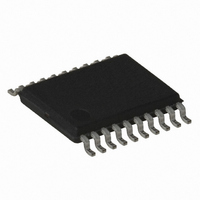
AT18F010-30XU Atmel, AT18F010-30XU Datasheet

AT18F010-30XU
Specifications of AT18F010-30XU
Related parts for AT18F010-30XU
AT18F010-30XU Summary of contents
Page 1
... The AT18F Series Configurators can be programmed with Atmel or industry-standard, third-party, stand-alone programmers such as BP, Data I/O, Hi-Lo, etc. AT18F002 AT18F040 AT18F080 2 Mbit 4 Mbit Yes 3.3V 1.8-3.3V 1.8-3.3V 33 MHz 20-lead TSSOP Yes FPGA Configuration Flash Memory AT18F010 AT18F002 AT18F040 AT18F080 Preliminary 7 Mbit 3672A–CNFG–1/08 ...
Page 2
... Pin Configuration 3. Block Diagram Power-on Reset Internal Oscillator Flash Memory AT18F010/002/040/080 [Preliminary] 2 20-lead TSSOP DATA CLK 3 18 TDI 4 17 TMS 5 16 TCK RESET/ Controller VCCJ VCCO VCCINT TDO CEO NC GND TCK TMS JTAG Interface TDI TDO CF CE Download RESET/OE Interface CEO ...
Page 3
... High after the RESET/OE reset pulse, the counter is reset and the DATA output pin is tri-stated. When the configurator has driven out all of its data and CEO is driven Low, the device tri-states the DATA pin to avoid contention with other configurators. Upon power-up, the address counter is automatically reset. 3672A–CNFG–1/08 AT18F010/002/040/080 [Preliminary] 3 ...
Page 4
... AT18F series devices are compatible with a portion of the Xilinx’s FGPA device families. Table 4-1. Atmel AT18F010-30XU AT18F002-30XU AT18F010/002/040/080 [Preliminary] 4 AT18F Series Configurator Compatibility with Xilinx FPGAs Xilinx XC2V40 Virtex-II XC2V80 XCV50E Virtex-E XCV100E XCV50 Virtex XCV100 XCV150 Spartan-3E XC3S100E XC3S50 ...
Page 5
... TDI pin while the output is directed to the TDO pin. Capture registers are used to capture active device data signals, to shift data in and out of the device and to load data into the update registers. Control signals are generated internally by the JTAG TAP controller. 3672A–CNFG–1/08 AT18F010/002/040/080 [Preliminary] 5 ...
Page 6
... This pin has an internal 20 KΩ pull-up resistor. 6.5 CF Configuration Pulse (open-drain output). Allows JTAG CONFIG instruction to initiate FPGA con- figuration without powering down the FPGA. This is an open-drain output that is pulsed Low by the JTAG CONFIG command. AT18F010/002/040/080 [Preliminary] 6 Pin Descriptions Type I ...
Page 7
... CE is asserted High. In this mode, the AT18F Configurator consumes less than current at 3.3V. The output remains in a high-impedance state regardless of the state of the OE input. 3672A–CNFG–1/08 AT18F010/002/040/080 [Preliminary] provides a logic 1 to the device. CCJ provides a logic 1 to the device if the pin is not driven. ...
Page 8
... Configuration Memory to FPGA Device Interface Connection Diagrams Figure 8-1. General Connection Diagram for Loading FPGA from Configurator and JTAG Signals Notes: 1. Signals within parenthesis will be applied to Atmel AT40AK FPGA. 2. For details of the circuit connection, please contact factory. AT18F010/002/040/080 [Preliminary] 8 3672A–CNFG–1/08 ...
Page 9
... Input Low Voltage IL V Input High Voltage IH 3672A–CNFG–1/08 AT18F010/002/040/080 [Preliminary] *NOTICE: Stresses beyond those listed under Absolute Maximum Ratings may cause permanent dam- age to the device. This is a stress rating only and functional operation of the device at these or any other conditions beyond those listed under oper- +0 ...
Page 10
... Output Drive Supply Current, Standby Mode CCIOS I JTAG Supply Current, Standby Mode CCJS I Input or I/O Low Leakage IL I Input or I/O High Leakage IH V Output Low Voltage OL V Output High Voltage OH AT18F010/002/040/080 [Preliminary] 10 Condition 33 MHz 33 MHz V = 3.6V, CCINT V = 3.6V CIO V = 3.6V, CCINT V = 3.6V CIO ...
Page 11
... HCE T RESET/OE Hold Time HOE T Block Erase Time BLKE Bulk Erase Time – 1M Bulk Erase Time – ERASE Bulk Erase Time – 4M Bulk Erase Time – TAP Clock Minimum Period CK_J 3672A–CNFG–1/08 AT18F010/002/040/080 [Preliminary] T CYC CAC T HCE T HOE T DF ...
Page 12
... RESET/OE CE CLK DATA LAST BIT CEO Table 12-2. AC Characteristics When Cascading Symbol Description T CLK to Output Float Delay CDF T CLK to CEO Delay OCK CEO Delay OCE T RESET/OE to CEO Delay OOE AT18F010/002/040/080 [Preliminary CDF T OCK FIRST BIT T OCE T OOE Min Max Units 3672A–CNFG–1/08 ...
Page 13
... Ordering Information Memory Size 1-Mbit 2-Mbit 4-Mbit 7-Mbit 20A2 20-lead, 0.65 mm Wide, Plastic Think-Shrink Small Outline (TSSOP) 3672A–CNFG–1/08 AT18F010/002/040/080 [Preliminary] Ordering Code AT18F010-30XU 20A2 - 20 TSSOP AT18F002-30XU 20A2 - 20 TSSOP AT18F040-30XU 20A2 - 20 TSSOP AT18F080-30XU 20A2 - 20 TSSOP Package Type Package Operation Range Industrial (-40° ...
Page 14
... Dambar cannot be located on the lower radius of the foot. Minimum space between protrusion and adjacent lead is 0.07 mm. 5. Dimension D and determined at Datum Plane H. 2325 Orchard Parkway 2325 Orchard Parkway San Jose, CA 95131 San Jose, CA 95131 R R AT18F010/002/040/080 [Preliminary Side View Pin1 Corner ...
Page 15
... Revision History Revision Level – Release Date A – January 2008 3672A–CNFG–1/08 AT18F010/002/040/080 [Preliminary] History Initial release. 15 ...
Page 16
... Disclaimer: The information in this document is provided in connection with Atmel products. No license, express or implied, by estoppel or otherwise, to any intellectual property right is granted by this document or in connection with the sale of Atmel products. EXCEPT AS SET FORTH IN ATMEL’S TERMS AND CONDI- TIONS OF SALE LOCATED ON ATMEL’S WEB SITE, ATMEL ASSUMES NO LIABILITY WHATSOEVER AND DISCLAIMS ANY EXPRESS, IMPLIED OR STATUTORY WARRANTY RELATING TO ITS PRODUCTS INCLUDING, BUT NOT LIMITED TO, THE IMPLIED WARRANTY OF MERCHANTABILITY, FITNESS FOR A PARTICULAR PURPOSE, OR NON-INFRINGEMENT ...


