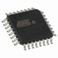
AT17LV010A-10QI Atmel, AT17LV010A-10QI Datasheet - Page 6

AT17LV010A-10QI
Manufacturer Part Number
AT17LV010A-10QI
Description
IC SRL CONFIG EEPROM 1M 32-TQFP
Manufacturer
Atmel
Datasheet
1.AT17LV512A-10JU.pdf
(18 pages)
Specifications of AT17LV010A-10QI
Programmable Type
Serial EEPROM
Memory Size
1Mb
Voltage - Supply
3 V ~ 3.6 V, 4.5 V ~ 5.5 V
Operating Temperature
-40°C ~ 85°C
Package / Case
32-TQFP
For Use With
ATDH2225 - CABLE ISP FOR AT17ATDH2200E - CONFIGURATOR PROGRAM BOARD KIT
Lead Free Status / RoHS Status
Contains lead / RoHS non-compliant
Available stocks
Company
Part Number
Manufacturer
Quantity
Price
4.10
4.11
4.12
5. FPGA Master Serial Mode Summary
6. Control of Configuration
7. Cascading Serial Configuration EEPROMs
6
READY
SER_EN
V
AT17LV65A/128A/256A/512A/002A
CC
Open collector reset state indicator. Driven Low during power-on reset cycle, released when
power-up is complete. (recommended 4.7 kΩ pull-up on this pin if used).
Serial enable must be held High during FPGA loading operations. Bringing SER_EN Low
enables the 2-wire Serial Programming Mode. For non-ISP applications, SER_EN should be tied
to V
3.3V (±10%) and 5.0V (±5% Commercial, ±10% Industrial) power supply pin.
The I/O and logic functions of any SRAM-based FPGA are established by a configuration pro-
gram. The program is loaded either automatically upon power-up, or on command, depending
on the state of the FPGA mode pins. In Master mode, the FPGA automatically loads the config-
uration program from an external memory. The AT17A Serial Configuration EEPROM has been
designed for compatibility with the Master Serial mode.
This document discusses the Altera FLEX FPGA device interfaces
Most connections between the FPGA device and the AT17A Serial EEPROM are simple and
self-explanatory.
For multiple FPGAs configured as a daisy-chain, or for FPGAs requiring larger configuration
memories, cascaded configurators provide additional memory.
After the last bit from the first configurator is read, the next clock signal to the configurator
asserts its nCASC output low and disables its DATA line driver. The second configurator recog-
nizes the low level on its nCS input and enables its DATA output.
After configuration is complete, the address counters of all cascaded configurators are reset if
the RESET/OE on each configurator is driven to a Low level.
If the address counters are not to be reset upon completion, then the RESET/OE input can be
tied to a High level.
The
• The DATA output of the AT17A series configurator drives DIN of the FPGA devices.
• The master FPGA DCLK output or external clock source drives the DCLK input of the AT17A
• The nCASC output of any AT17A series configurator drives the nCS input of the next
• SER_EN must be connected to V
series configurator.
configurator in a cascaded chain of EEPROMs.
CC
AT17LV65A devices do not have the
.
CC
(except during ISP).
nCASC feature to perform cascaded configurations.
2322G–CNFG–03/06


