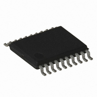
AT18F040-30XU Atmel, AT18F040-30XU Datasheet - Page 5

AT18F040-30XU
Manufacturer Part Number
AT18F040-30XU
Description
IC FLASH CONFIG 4MBIT 20-TSSOP
Manufacturer
Atmel
Datasheet
1.AT18F010-30XU.pdf
(16 pages)
Specifications of AT18F040-30XU
Programmable Type
FLASH
Memory Size
4Mb
Voltage - Supply
3 V ~ 3.6 V
Operating Temperature
-40°C ~ 85°C
Package / Case
20-TSSOP (0.173", 4.40mm Width)
Lead Free Status / RoHS Status
Lead free / RoHS Compliant
5. Programming
5.1
5.2
3672A–CNFG–1/08
JTAG-BST Overview
JTAG Boundary-scan Cell (BSC) Testing
AT18Fxx devices are in-system programmable (ISP) devices utilizing the 4-pin JTAG protocol.
This capability eliminates package handling normally required for programming and facilitates
rapid design iterations and field changes.
Atmel provides ISP hardware and software to allow programming of the AT18Fxx via the PC.
ISP is performed by using either a download cable or a comparable board tester or a simple
microprocessor interface.
To allow ISP programming support by the Automated Test Equipment (ATE) vendors, Serial
Vector Format (SVF) files can be created by the Atmel JCPS Software. Conversion to other ATE
tester format beside SVF is also possible
AT18Fxx devices can also be programmed using standard third-party programmers such as BP,
DataI/O, Hi-Lo, etc. Factory-preprogrammed devices, as required by customers, are also avail-
able for certain ordering quantities.
Contact your local Atmel representatives or Atmel PLD applications for details.
The JTAG boundary-scan testing is controlled by the Test Access Port (TAP) controller in the
AT18F series. The boundary-scan technique involves the inclusion of a shift-register stage (con-
tained in a boundary-scan cell) adjacent to each component so that signals at component
boundaries can be controlled and observed using scan testing principles. Each input pin and I/O
pin has its own boundary-scan cell (BSC) in order to support boundary-scan testing. The
AT18Fxx series does not currently include a Test Reset (TRST) input pin because the TAP con-
troller is automatically reset at power-up. The six JTAG BST modes supported include:
SAMPLE/PRELOAD, EXTEST, BYPASS and IDCODE. BST on the AT18Fxx series is imple-
mented using the Boundary-scan Definition Language (BSDL) described in the JTAG
specification (IEEE Standard 1149.1). Any third-party tool that supports the BSDL format can be
used to perform BST on the AT18Fxx series.
The AT18F series uses the four JTAG-standard I/O pins for In-System programming (ISP). The
AT18F series is programmable through the four JTAG pins using programming algorithm com-
patible with the IEEE JTAG Standard 1532. Programming is performed by using selectable
voltage levels of the programming signals from the JTAG ISP interface.
The AT18F series has I/Os that contain boundary-scan cells (BSC) in order to support bound-
ary-scan testing as described in detail by IEEE Standard 1149.1. Input to the capture register
chain is fed in from the TDI pin while the output is directed to the TDO pin. Capture registers are
used to capture active device data signals, to shift data in and out of the device and to load data
into the update registers. Control signals are generated internally by the JTAG TAP controller.
AT18F010/002/040/080 [Preliminary]
5


