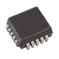
AT17LV010-10JI Atmel, AT17LV010-10JI Datasheet - Page 6

AT17LV010-10JI
Manufacturer Part Number
AT17LV010-10JI
Description
IC SRL CONFIG EEPROM 1M 20-PLCC
Manufacturer
Atmel
Datasheet
1.AT17LV65-10CC.pdf
(26 pages)
Specifications of AT17LV010-10JI
Programmable Type
Serial EEPROM
Memory Size
1Mb
Voltage - Supply
3 V ~ 3.6 V, 4.5 V ~ 5.5 V
Operating Temperature
-40°C ~ 85°C
Package / Case
20-LCC (J-Lead)
For Use With
ATDH2225 - CABLE ISP FOR AT17ATDH2200E - CONFIGURATOR PROGRAM BOARD KIT
Lead Free Status / RoHS Status
Contains lead / RoHS non-compliant
Other names
AT17LV01010JI
Available stocks
Company
Part Number
Manufacturer
Quantity
Price
Part Number:
AT17LV010-10JI
Manufacturer:
ATMEL/爱特梅尔
Quantity:
20 000
3. Device Description
4. Pin Description
Note:
6
RESET/OE
SER_EN
READY
Name
DATA
WP1
WP2
GND
CEO
CLK
V
CE
A2
CC
1. The CEO feature is not available on the AT17LV65 device.
AT17LV65/128/256/512/010/002/040
I/O
I/O
O
O
I
I
I
I
I
I
I
SOIC
LAP/
DIP/
8
1
2
–
3
4
5
6
–
7
8
The control signals for the configuration EEPROM (CE, RESET/OE and CCLK) interface directly
with the FPGA device control signals. All FPGA devices can control the entire configuration pro-
cess and retrieve data from the configuration EEPROM without requiring an external intelligent
controller.
The configuration EEPROM RESET/OE and CE pins control the tri-state buffer on the DATA
output pin and enable the address counter. When RESET/OE is driven High, the configuration
EEPROM resets its address counter and tri-states its DATA pin. The CE pin also controls the
output of the AT17LV series configurator. If CE is held High after the RESET/OE reset pulse, the
counter is disabled and the DATA output pin is tri-stated. When OE is subsequently driven Low,
the counter and the DATA output pin are enabled. When RESET/OE is driven High again, the
address counter is reset and the DATA output pin is tri-stated, regardless of the state of CE.
When the configurator has driven out all of its data and CEO is driven Low, the device tri-states
the DATA pin to avoid contention with other configurators. Upon power-up, the address counter
is automatically reset.
This is the default setting for the device. Since almost all FPGAs use RESET Low and OE High,
this document will describe RESET/OE.
AT17LV128/
AT17LV256
AT17LV65/
PLCC
20
10
14
17
20
2
4
–
6
8
–
SOIC
20
10
14
17
20
2
4
–
6
8
–
DIP/
LAP
8
1
2
–
3
–
4
5
6
–
7
8
AT17LV512/
AT17LV010
PLCC
20
10
14
15
17
20
2
4
5
6
7
8
SOIC
20
10
11
13
18
20
1
3
–
8
–
–
–
SOIC
LAP/
DIP/
8
1
2
–
3
–
4
5
6
–
7
8
PLCC
20
10
14
15
17
20
2
4
5
6
7
8
AT17LV002
SOIC
20
10
11
13
18
20
1
3
–
8
–
–
–
TQFP
44
40
43
13
15
18
21
23
35
38
–
–
2321I–CNFG–2/08
AT17LV040
TQFP
44
40
43
13
15
18
21
35
38
23
–
–


