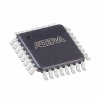
EPC1441TC32N Altera, EPC1441TC32N Datasheet - Page 21

EPC1441TC32N
Manufacturer Part Number
EPC1441TC32N
Description
IC CONFIG DEVICE 440KBIT 32-TQFP
Manufacturer
Altera
Series
EPCr
Datasheet
1.EPC1PC8.pdf
(26 pages)
Specifications of EPC1441TC32N
Programmable Type
OTP
Memory Size
440kb
Voltage - Supply
3 V ~ 3.6 V, 4.75 V ~ 5.25 V
Operating Temperature
0°C ~ 70°C
Package / Case
32-TQFP, 32-VQFP
Lead Free Status / RoHS Status
Lead free / RoHS Compliant
Other names
544-1649
Available stocks
Company
Part Number
Manufacturer
Quantity
Price
Company:
Part Number:
EPC1441TC32N
Manufacturer:
VIALTA
Quantity:
1 440
Part Number:
EPC1441TC32N
Manufacturer:
ALTERA/阿尔特拉
Quantity:
20 000
Chapter 4: Configuration Devices for SRAM-Based LUT Devices Data Sheet
Pin Information
Pin Information
Table 4–20. EPC1, EPC2 and EPC1441 Pin Functions During Configuration (Part 1 of 3)
© December 2009
DATA
DCLK
OE
Pin Name
f
f
Altera Corporation
PDIP
8-Pin
1
2
3
Table 4–20
configuration.
For pin information about enhanced configuration devices, refer to the
Configuration Devices (EPC4, EPC8 and EPC16) Data
For pin information about serial configuration devices, refer to the
Devices (EPCS1, EPCS4, EPCS16, EPCS64 and EPCS128) Data
(1)
Pin Number
20-Pin
PLCC
2
4
8
describes EPC1, EPC2, and EPC1441 pin functions during device
TQFP
32-Pin
31
2
7
(2)
Output
Bidirectional
Open-Drain
Bidirectional
Pin Type
Serial data output. The DATA pin connects to the
DATA0 of the FPGA. DATA is latched into the FPGA
on the rising edge of DCLK.
The DATA pin is tri-stated before configuration and
when the nCS pin is high. After configuration, the
EPC2 device will drive DATA high, while the EPC1
and EPC1441 device will tri-state DATA.
Clock output when configuring with a single
configuration device or when the configuration
device is the first (master) device in a chain. Clock
input for the next (slave) configuration devices in a
chain. The DCLK pin connects to the DCLK of the
FPGA.
Rising edges on DCLK increment the internal
address counter and present the next bit of data on
the DATA pin. The counter is incremented only if the
OE input is held high, the nCS input is held low, and
all configuration data has not been transferred to the
target device.
After configuration or when OE is low, the EPC1,
EPC2 and EPC1441 device will drive DCLK low.
Output enable (active high) and reset (active low).
The OE pin connects to the nSTATUS of the FPGA.
A low logic level resets the address counter. A high
logic level enables DATA and the address counter to
count. If this pin is low (reset) during configuration,
the internal oscillator becomes inactive and DCLK
drives low. Refer to
page
The OE pin has an internal programmable 1-k
resistor in EPC2 devices. If internal pull-up resistors
are use, external pull-up resistors should not be used
on these pins. The internal pull-up resistors can be
disabled through the Disable nCS and OE pull-ups
on configuration device option.
4–9.
Configuration Handbook (Complete Two-Volume Set)
Sheet.
“Error Detection Circuitry” on
Description
Sheet.
Serial Configuration
Enhanced
4–21


