AT17C512A-10JI Atmel, AT17C512A-10JI Datasheet
AT17C512A-10JI
Specifications of AT17C512A-10JI
Available stocks


Related parts for AT17C512A-10JI


AT17C512A-10JI Summary of contents
Page 1
... Available in 3.3V ± 10% LV and 5V ± Versions • System-friendly READY Pin Description The AT17C512A/010A and AT17LV512A/010A (high-density AT17A Series) FPGA Configuration EEPROMs (Configurators) provide an easy-to-use, cost-effective con- figuration memory for programming Altera FLEX devices are packaged in the popular 8-lead PDIP and the 20-lead PLCC; the AT17C010A/LV010A are packaged in the popular 8-lead PDIP, the 20-lead PLCC and the 32-lead TQFP ...
Page 2
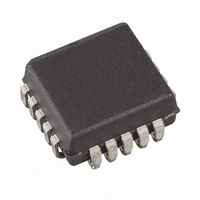
... Pin Configuration 8-lead PDIP DATA 1 8 DCLK nCS DCLK NC WP1 Note: 1. The 32-lead TQFP package is not available for AT17C512A/LV512A devices. AT17C/LV512A/010A 2 VCC SER_EN (A2) nCASC GND (1) 32-lead TQFP 20-lead PLCC 18 SER_EN DCLK 4 WP1 READY SER_EN NC NC READY 0974E–08/01 ...
Page 3
Block Diagram SER_EN WP1 OSC CONTROL OSC POWER ON RESET DCLK READY (Optional) Device Configuration 0974E–08/01 PROGRAMMING MODE LOGIC ROW ADDRESS COUNTER BIT COUNTER OE nCS The control signals for the configuration EEPROM (nCS, OE and DCLK) interface directly with ...
Page 4
FPGA Device Configuration AT17C/LV512A/010A 4 The READY pin is available as an open-collector indicator of the device’s reset status driven Low while the device is in its power-on reset cycle and released (tri-stated) when the cycle is complete. ...
Page 5
... Introducing an RC delay to the input of nCONFIG is recommended to ensure that V configuration begins. (nCONFIG can instead be connected to an active Low system reset signal.) 3. Reset polarity of EEPROM must be set active Low (OE active High) 0974E–08/01 AT17C/LV512A/010A (1)(2)( AT17C512A/010A/020A AT17LV512A/010A/020A DCLK SER_EN DATA nCS OE READY (5V/3.3V) is reached before CC 5 ...
Page 6
... The AT17A Series Configurator enters a low-power standby mode whenever nCS is asserted High. In this mode, the configuration consumes less than 0 current at 5V. The output remains in a high-impedance state regardless of the state of the OE input. AT17C512A/010A/020A AT17LV512A/010A/020A DEVICE 2 DCLK SER_EN ...
Page 7
Pin Configurations PDIP PLCC TQFP Pin Pin Pin Name DATA DCLK 5 4 WP1 nCS GND nCASC ...
Page 8
Absolute Maximum Ratings* Operating Temperature.................................. -55°C to +125°C Storage Temperature ..................................... -65°C to +150°C Voltage on Any Pin with Respect to Ground ..............................-0. Supply Voltage (V ) .........................................-0.5V to +7.0V CC Maximum Soldering Temp. (10 sec @ 1/16 ...
Page 9
... Low-level Output Voltage ( High-level Output Voltage ( Low-level Output Voltage ( Supply Current, Active Mode (at FMAX) CCA I Input or Output Leakage Current ( Supply Current, Standby Mode AT17C512A/010A CCS DC Characteristics V = 3.3V ± 10% CC Symbol Description V High-level Input Voltage IH V Low-level Input Voltage IL V High-level Output Voltage (I ...
Page 10
AC Characteristics nCS T OE DCLK DATA AC Characteristics When Cascading OE nCS DCLK T CDF LAST BIT DATA T OCK nCASL AT17C/LV512A/010A 10 SCE CAC T OCE T SCE T ...
Page 11
... DCLK High Time Master Mode HC Notes: 1. Preliminary specifications for military operating range only test load = 50 pF. 3. Float delays are measured with loads. Transition is measured ±=200 mV from steady state active levels. AC Characteristics for AT17C512A/010A When Cascading ± 5% Commercial ± 10% Industrial/Military CC CC ...
Page 12
AC Characteristics for AT17LV512A/010A V = 3.3V ± 10% Commercial Symbol Description ( Data Delay OE (2) T nCS to Data Delay CE (2) T DCLK to Data Delay CAC T Data Hold From nCS, ...
Page 13
... Ordering Information – 5V Devices Memory Size Ordering Code (1) 512-Kbit AT17C512A-10PC AT17C512A-10JC AT17C512A-10PI AT17C512A-10JI (2) 1-Mbit AT17C010A-10PC AT17C010A-10JC AT17C010A-10QC AT17C010A-10PI AT17C010A-10JI AT17C010A-10QI Notes: 1. Use 512-Kbit density parts to replace Altera EPC1441. 2. Use 1-Mbit density parts to replace Altera EPC1. Ordering Information – 3.3V Devices Memory ...
Page 14
Packaging Information 8P3, 8-lead, 0.300” Wide, Plastic Dual Inline Package (PDIP) Dimensions in Inches and (Millimeters) JEDEC STANDARD MS-018 AA 32A, 32-lead, Thin (1.0 mm) Plastic Gull Wing Quad Flat package (TQFP) Dimensions in Millimeters and (Inches) PIN 1 ID ...
Page 15
... No licenses to patents or other intellectual property of Atmel are granted by the Company in connection with the sale of Atmel products, expressly or by implication. Atmel’s products are not authorized for use as critical components in life support devices or systems. ...