AT17F080-30JC Atmel, AT17F080-30JC Datasheet
AT17F080-30JC
Specifications of AT17F080-30JC
Available stocks


Related parts for AT17F080-30JC


AT17F080-30JC Summary of contents
Page 1
... AT17F Series Packages Package 8-lead LAP 20-lead PLCC 44-lead TQFP ® ® FLEX , APEX XC3000, XC4000, XC5200, Spartan AT17F040 Yes Yes – FPGA ™ Devices, ® ® , Virtex FPGAs, Configuration Flash Memory AT17F040 AT17F080 AT17F080 Yes Yes Yes 3039K–CNFG–2/08 ...
Page 2
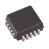
Pin Configuration Notes: AT17F040/080 2 8-lead LAP DATA 1 8 VCC CLK 2 7 SER_EN RESET/ CEO (A2 GND 20-lead PLCC CLK RESET/OE 6 PAGESEL1 20-lead PLCC (Virtex ...
Page 3
3039K–CNFG–2/08 44 TQFP AT17F040/080 ...
Page 4
Block Diagram Power-on READY Reset PAGE_EN Config. Page PAGESEL0 Select PAGESEL1 Flash Memory 4. Device Description The control signals for the configuration memory device (CE, RESET/OE and CLK) interface directly with the FPGA device control signals. All FPGA devices ...
Page 5
... AT17F040 20 PLCC 8 20 LAP PLCC (Virtex – 16 – – 11 – – 7 – – This pin has an internal 20 KΩ pull-up resistor. 2. This pin has an internal 30 KΩ pull-down resistor. AT17F040/080 AT17F080 LAP PLCC TQFP – – – – ...
Page 6
... This pin has an internal 20 kΩ pull-up resistor. 2. This pin has an internal 30 kΩ pull-down resistor. Table 5-2. When AT17F080 (8 Mbits) 00000 – 1FFFFh 20000 – 3FFFFh 40000 – 5FFFFh 60000 – 7FFFFh 00000 – 7FFFFh and GND is recommended ...
Page 7
... A2 Device selection input, (when SER_EN Low). The input is used to enable (or chip select) the device during programming (i.e., when SER_EN is Low). Refer to the AT17F Programming Specification available on the Atmel web site for additional details. 5.10 READY Open collector reset state indicator. Driven Low during power-up reset, released when power-up is complete. (recommended 4.7 kΩ ...
Page 8
... FPGA mode pins. In Master mode, the FPGA automatically loads the config- uration program from an external memory. The AT17F Serial Configuration PROM has been designed for compatibility with the Master Serial mode. This document discusses the Atmel AT40K, AT40KAL and AT94KAL applications as well as Xil- inx applications. 7. Control of Configuration Most connections between the FPGA device and the AT17F Serial Configurator PROM are sim- ple and self-explanatory ...
Page 9
... Exposure to Abso- lute Maximum Rating conditions for extended periods of time may affect device reliability. AT17F Series Configurator Min Max 2.97 3.63 2.97 3.63 AT17F040 AT17F080 Min Max Min 2 0.8 0 2.4 2 ...
Page 10
AC Characteristics CE RESET/OE CLK T CE DATA 15. AC Characteristics when Cascading RESET/OE CE CLK T DATA LAST BIT T CEO AT17F040/080 10 T SCE CAC CDF T OCK OCE T ...
Page 11
AC Characteristics Symbol Description ( Data Delay OE ( Data Delay CE (2) T CLK to Data Delay CAC T Data Hold from CE, OE, or CLK OH ( ...
Page 12
... Maximum Input Clock Frequency MAX Notes test lead = 50 pF. 2. Float delays are measured with loads. Transition is measured ± 200 mV from steady-state active levels. AT17F040/080 12 AT17F040 Min Commercial Industrial Commercial Industrial Commercial Industrial Commercial Industrial Commercial Industrial AT17F080 Max Min Max Units ...
Page 13
... Plastic Leaded Chip Carrier (PLCC) 44A Thin Plastic Quad Flat Package (TQFP) Note: 1. Airflow = 0 ft/min. 3039K–CNFG–2/08 AT17F040 θ [° C/W] JC θ (1) [° C/W] JA θ [° C/W] JC θ (1) [° C/W] JA θ [° C/W] – JC θ (1) [° C/W] – JA AT17F040/080 AT17F080 – – – – ...
Page 14
... Thin (1.0 mm) Plastic Quad Flat Package Carrier (TQFP) AT17F040/080 14 Ordering Code AT17F040-30VJC AT17F040-30VJI AT17F080-30TQC AT17F080-30TQI Ordering Code AT17F040-30CU AT17F040-30JU AT17F080-30CU AT17F080-30JU Package Type (1)(2) Package Operation Range Commercial 20J - 20 PLCC (0° 70° C) Industrial 20J - 20 PLCC (-40° 85° C) Commercial 44A - 44 TQFP (0° ...
Page 15
... TYP Bottom View Note: 1. Metal Pad Dimensions. 2. All exposed metal area shall have the following finished platings. Ni: 0.0005 to 0.015 mm Au: 0.0005 to 0.001 mm Package Drawing Contact: packagedrawings@atmel.com 3039K–CNFG–2/08 D Pin1 Corner TITLE 8CN4, 8-lead ( 1.04 mm Body), Lead Pitch 1.27mm, Leadless Array Package (LAP) ...
Page 16
PLCC 1.14(0.045) X 45˚ B 0.51(0.020)MAX 45˚ MAX (3X) Notes: 1. This package conforms to JEDEC reference MS-018, Variation AA. 2. Dimensions D1 and E1 do not include mold protrusion. Allowable protrusion is .010"(0.254 mm) per side. ...
Page 17
TQFP PIN 0˚~7˚ L Notes: 1. This package conforms to JEDEC reference MS-026, Variation ACB. 2. Dimensions D1 and E1 do not include mold protrusion. Allowable protrusion is 0.25 mm per side. Dimensions D1 ...
Page 18
Revision History Revision Level – Release Date J – March 2006 K – February 2008 AT17F040/080 18 History Added last-time buy for AT17FXXX-30CC and AT17FXXX-30CI. Removed -30JC, -30JI, -30BJC and -30BJI devices from ordering information. 3039K–CNFG–2/08 ...
Page 19
... Disclaimer: The information in this document is provided in connection with Atmel products. No license, express or implied, by estoppel or otherwise, to any intellectual property right is granted by this document or in connection with the sale of Atmel products. EXCEPT AS SET FORTH IN ATMEL’S TERMS AND CONDI- TIONS OF SALE LOCATED ON ATMEL’S WEB SITE, ATMEL ASSUMES NO LIABILITY WHATSOEVER AND DISCLAIMS ANY EXPRESS, IMPLIED OR STATUTORY WARRANTY RELATING TO ITS PRODUCTS INCLUDING, BUT NOT LIMITED TO, THE IMPLIED WARRANTY OF MERCHANTABILITY, FITNESS FOR A PARTICULAR PURPOSE, OR NON-INFRINGEMENT ...