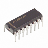
DS1321 Maxim Integrated Products, DS1321 Datasheet

DS1321
Specifications of DS1321
Available stocks
Related parts for DS1321
DS1321 Summary of contents
Page 1
... V 2 BAT TOL 3 CEI1 4 CEI2 5 A/CEI3 6 B/CEI4 7 GND 8 DS1321S 16-Pin SOIC (150-mil CCO V 2 BAT TOL 3 CEI1 4 CEI2 A/CEI3 7 B/CEI4 GND DS1321E 20-Pin TSSOP DS1321 16 V CCI 15 RST CEO1 12 CEO2 11 CEO3 10 CEO4 9 MODE 16 V CCI 15 RST CEO1 12 CEO2 11 CEO3 10 CEO4 9 MODE 20 V ...
Page 2
... As a result, the Battery Warning pin is activated to signal the need for battery replacement. MEMORY BACKUP The DS1321 performs all the circuit functions required to provide battery-backup for as many as four SRAMs. First, the device provides a switch to direct power from the battery or the system power supply (V ) ...
Page 3
... MEMORY CONFIGURATIONS The DS1321 can be configured via the MODE pin for three different arrangements of the four attached SRAMs. The state of the MODE pin is latched at V MEMORY CONFIGURATIONS Figure 1 MODE = GND (4 BANKS WITH 1 SRAM EACH): MODE = V (2 BANKS WITH 2 SRAM EACH): CCO ...
Page 4
... NOTE: The DS1321 cannot constantly monitor an attached battery because such monitoring would drastically reduce the life of the battery result, the DS1321 only tests the battery for one second out of every 24 hours and does not monitor the battery in any way between tests good battery (one that ...
Page 5
... FRESHNESS SEAL MODE When the battery is first attached to the DS1321 without V immediately provide battery-backup power on V leave Freshness Seal Mode. This mode allows a battery to be attached during manufacturing but not used until after the system has been activated for the first time result, no battery energy is drained during storage and shipping ...
Page 6
ABSOLUTE MAXIMUM RATINGS* Voltage on Any Pin Relative to Ground Operating Temperature Storage Temperature Soldering Temperature * This is a stress rating only and functional operation of the device at these or any other conditions above those indicated in the ...
Page 7
CAPACITANCE PARAMETER Input Capacitance ( *, TOL, MODE) CEI Output Capacitance ( *, , ) CEO BW RST AC ELECTRICAL CHARACTERISTICS PARAMETER to Propagation Delay CEI CEO Pulse Width CE V Valid to End of CC Write Protection V Valid ...
Page 8
TIMING DIAGRAM: POWER-UP NOTE > will begin to slew with V BAT CCTP CCO when CCI CCI CCTP ...
Page 9
TIMING DIAGRAM: POWER-DOWN NOTES > will slew down with V BAT CCTP CCO until CCI CCI CCTP ...
Page 10
TIMING DIAGRAM: BATTERY WARNING DETECTION NOTE measured from the expiration of the internal timer to the activation of the battery warning output TIMING DIAGRAM: BATTERY REPLACEMENT ...
Page 11
... DS1321 can supply to attached memories at V CCO2 V -0.3V. CCI 5. All inputs within 0.3V of ground the maximum average load current which the DS1321 can supply to the memories in the CCO3 battery backup mode Measured with a load as shown in Figure 1. 8. Chip Enable Outputs CEO1 9. ...
Page 12
... The following represent the key differences between 06/12/97 and 09/29/97 version of the DS1321 data sheet. Please review this summary carefully. 1. Changed AC test conditions The following represent the key differences between 09/29/97 and 12/12/97 version of the DS1321 data sheet. Please review this summary carefully. 1. Removed preliminary from title bar. ...


