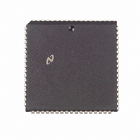
DP8421ATVX-25 National Semiconductor, DP8421ATVX-25 Datasheet - Page 42

DP8421ATVX-25
Manufacturer Part Number
DP8421ATVX-25
Description
IC CTRLR/DVR CMOS PROGRAM 68PLCC
Manufacturer
National Semiconductor
Datasheet
1.DP8420AV-25.pdf
(58 pages)
Specifications of DP8421ATVX-25
Controller Type
Dynamic RAM (DRAM)
Voltage - Supply
4.5 V ~ 5.5 V
Operating Temperature
0°C ~ 70°C
Package / Case
68-PLCC
Lead Free Status / RoHS Status
Contains lead / RoHS non-compliant
Other names
*DP8421ATVX-25
Available stocks
Company
Part Number
Manufacturer
Quantity
Price
Company:
Part Number:
DP8421ATVX-25
Manufacturer:
Texas Instruments
Quantity:
10 000
13 0 AC Timing Parameters
Two speed selections are given the DP8420A 21A 22A-20
and the DP8420A 21A 22A-25 The differences between
the two parts are the maximum operating frequencies of the
input CLKs and the maximum delay specifications Low fre-
quency applications may use the ‘‘
proved timing
The AC timing parameters are grouped into sectional num-
bers as shown below These numbers also refer to the tim-
ing diagrams
1 –36
50 –56
100 –121 Common dual access parameters used for Port
200 –212 Refresh parameters
Note 1 ‘‘Absolute Maximum Ratings’’ are the values beyond which the safety of the device cannot be guaranteed They are not meant to imply that the device
should be operated at these limits The table of ‘‘Electrical Characteristics’’ provides conditions for actual device operation
Note 2 Input pulse 0V to 3V tR
Note 3 AC Production testing is done at 50 pF
Common parameters to all modes of operation
Difference parameters used to calculate
RAS low time
RAS precharge time
CAS high time and
CAS low time
B accesses and inputs and outputs used only in
dual accessing
e
tF
e
2 5 ns Input reference point on AC measurements is 1 5V Output reference points are 2 4V for High and 0 8V for Low
b
25’’ part to gain im-
FIGURE 36 Clock DELCLK Timing
42
300 – 315 Mode 0 access parameters used in both single
400 – 416 Mode 1 access parameters used in both single
450 – 455 Special Mode 1 access parameters which super-
500 – 506 Programming parameters
Unless otherwise stated V
70 C the output load capacitance is typical for 4 banks of
18 DRAMs per bank including trace capacitance (see Note
2)
Two different loads are specified
C
C
C
C
C
L
L
H
H
H
e
e
e
e
e
50 pF loads on all outputs except
150 pF loads on Q0– 8 9 10 and WE or
50 pF loads on all outputs except
125 pF loads on RAS0– 3 and CAS0–3 and
380 pF loads on Q0– 8 9 10 and WE
and dual access applications
and dual access applications
sede the 400– 416 parameters when dual ac-
cessing
CC
e
5 0V
TL F 8588 – E9
g
10% 0
k
T
A k


