VIPER16LN STMicroelectronics, VIPER16LN Datasheet - Page 4
VIPER16LN
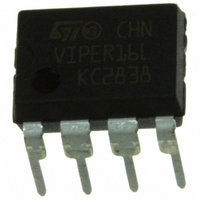
Manufacturer Part Number
VIPER16LN
Description
IC OFFLINE CONV PWM OVP OCP 7DIP
Manufacturer
STMicroelectronics
Series
VIPer™ plusr
Datasheet
1.VIPER16HDTR.pdf
(24 pages)
Specifications of VIPER16LN
Output Isolation
Either
Frequency Range
54 ~ 66kHz
Voltage - Input
11.5 ~ 23.5 V
Voltage - Output
800V
Power (watts)
12W
Operating Temperature
-40°C ~ 150°C
Package / Case
8-DIP (0.300", 7.62mm), 7 Leads
Output Voltage
800 V
Output Power
1 W
Input Voltage
- 0.3 V
Switching Frequency
115 KHz
Operating Temperature Range
- 40 C to + 150 C
Mounting Style
Through Hole
Duty Cycle (max)
80 %
Number Of Outputs
1
For Use With
497-9006 - BOARD EVAL BASED ON VIPER16497-8838 - EVAL BOARD FOR VIPER16LD497-8837 - EVAL BOARD FOR VIPER16LD ISO PSU
Lead Free Status / RoHS Status
Lead free / RoHS Compliant
Other names
497-8546-5
Available stocks
Company
Part Number
Manufacturer
Quantity
Price
Company:

Part Number:
VIPER16LN
Manufacturer:
PANASONIC
Quantity:
20 000
Part Number:
VIPER16LN
Manufacturer:
ST
Quantity:
20 000


Pin settings
3
Note:
4/24
Pin settings
Figure 3.
The copper area for heat dissipation has to be designed under the DRAIN pins.
Table 3.
DIP-7
7,8
1
2
3
4
5
-
Pin N.
SO16
13-16
1-2
Connection diagram (top view)
Pin description
4
5
6
7
8
DRAIN
COMP
Name
GND
VDD
N.A.
LIM
FB
Connected to the source of the internal power MOSFET and controller
ground reference.
Not available for user. It can be connected to GND (pins 1-2) or left not
connected.
Supply voltage of the control section. This pin provides the charging
current of the external capacitor.
This pin allows setting the drain current limitation. The limit can be
reduced by connecting an external resistor between this pin and GND.
Pin left open if default drain current limitation is used.
Inverting input of the internal trans conductance error amplifier.
Connecting the converter output to this pin through a single resistor
results in an output voltage equal to the error amplifier reference
voltage (See V
required for higher output voltages.
Output of the internal trans conductance error amplifier. The
compensation network have to be placed between this pin and GND to
achieve stability and good dynamic performance of the voltage control
loop. The pin is used also to directly control the PWM with an
optocoupler. The linear voltage range extends from V
V
High voltage drain pin. The built-in high voltage switched start-up bias
current is drawn from this pin too.
Pins connected to the metal frame to facilitate heat dissipation.
COMPH
Doc ID 15232 Rev 4
(Table
FB_REF
7).
on
Table
Function
7). An external resistors divider is
COMPL
to
VIPER16
Related parts for VIPER16LN
Image
Part Number
Description
Manufacturer
Datasheet
Request
R

Part Number:
Description:
IC OFFLINE CONV PWM OVP OCP 8DIP
Manufacturer:
STMicroelectronics
Datasheet:

Part Number:
Description:
IC OFFLINE SWIT PWM SMPS CM 8DIP
Manufacturer:
STMicroelectronics
Datasheet:
Part Number:
Description:
IC OFFLINE SWIT PWM SMPS 8DIP
Manufacturer:
STMicroelectronics
Datasheet:
Part Number:
Description:
IC OFFLINE SWIT PWM CM OTP 8DIP
Manufacturer:
STMicroelectronics
Datasheet:

Part Number:
Description:
IC SWIT PWM SMPS CM PENTAWATT5
Manufacturer:
STMicroelectronics
Datasheet:

Part Number:
Description:
IC SWIT PWM SMPS CM PENTAWATT5
Manufacturer:
STMicroelectronics
Datasheet:

Part Number:
Description:
IC OFFLINE SWIT PWM SMPS 8SOIC
Manufacturer:
STMicroelectronics
Datasheet:

Part Number:
Description:
IC OFFLINE SWIT PWM POWERSO10
Manufacturer:
STMicroelectronics
Datasheet:

Part Number:
Description:
IC OFFLINE CONV PWM OVP 8DIP
Manufacturer:
STMicroelectronics
Datasheet:
Part Number:
Description:
IC SWIT SMPS CM OTP PENTAWATT5
Manufacturer:
STMicroelectronics
Datasheet:
Part Number:
Description:
IC SWIT PWM SMPS CM PENTAWATT5
Manufacturer:
STMicroelectronics
Datasheet:

Part Number:
Description:
IC OFFLINE CONV PWM OTP 16-SOIC
Manufacturer:
STMicroelectronics
Datasheet:
Part Number:
Description:
IC OFFLINE CONV PWM OTP 16-SOIC
Manufacturer:
STMicroelectronics
Datasheet:
Part Number:
Description:
IC OFFLINE SWIT PWM SMPS 8SOIC
Manufacturer:
STMicroelectronics
Datasheet:

Part Number:
Description:
IC OFFLINE CONV PWM OVP OCP 8DIP
Manufacturer:
STMicroelectronics
Datasheet: