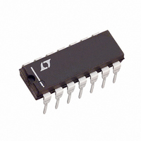
LT1105IN Linear Technology, LT1105IN Datasheet - Page 24

LT1105IN
Manufacturer Part Number
LT1105IN
Description
IC OFFLINE SWIT CM HV 14DIP
Manufacturer
Linear Technology
Datasheet
1.LT1105CN8PBF.pdf
(32 pages)
Specifications of LT1105IN
Output Isolation
Isolated
Frequency Range
20 ~ 200kHz
Voltage - Input
7 ~ 30 V
Voltage - Output
20V
Power (watts)
100W
Operating Temperature
-40°C ~ 125°C
Package / Case
14-DIP (0.300", 7.62mm)
Lead Free Status / RoHS Status
Contains lead / RoHS non-compliant
Available stocks
Company
Part Number
Manufacturer
Quantity
Price
Part Number:
LT1105IN
Manufacturer:
LINEAR/凌特
Quantity:
20 000
Part Number:
LT1105IN#PBF
Manufacturer:
LINEAR/凌特
Quantity:
20 000
Company:
Part Number:
LT1105IN8#PBF
Manufacturer:
LINEAR
Quantity:
29
Part Number:
LT1105IN8#PBF
Manufacturer:
LINEAR/凌特
Quantity:
20 000
APPLICATIONS
LT1103/LT1105
compensation can be set to cancel the effects of these
parasitic voltage drops. The feature can be ignored by
eliminating the series resistor and lowering the equivalent
divider impedance to swamp out the effects of the input
bias current.
Frequency Compensation
In order to prevent a regulator loop using the LT1103/
LT1105 from oscillating, frequency compensation is
required. Although the architecture of the LT1103/LT1105
is simple enough to lend itself to a mathematical approach
to frequency compensation, the added complication of
input/or output filters, unknown capacitor ESR, and gross
operating point changes with input voltage and load current
variations all suggest a more practical empirical approach.
Many hours spent on breadboards have shown that the
simplest way to optimize the frequency compensation of
the LT1103/LT1105 is to use transient response techniques
and an “RC” box to quickly iterate toward the final
compensation network. Additional information on this
technique of frequency compensation can be found in
Linear Technology’s Application Note 19.
In general, frequency compensation is accomplished with
an RC series network on the V
a g
Voltage gain is determined by multiplying g
total equivalent error amplifier output loading, consisting
of the error amplifier output impedance in parallel with the
series RC external frequency compensation network. At
DC, the external RC can be ignored. The output impedance
of the error amplifier is typically 100k
voltage gain of 1200V/V. At frequencies just above DC,
the voltage gain is determined by the external
compensation, R
given by:
The gain at high frequencies is given by:
Phase shift from the FB pin to the V
frequencies where the external C
24
A
m
A
V
V
(voltage “in” to current “out”) of
= g
2 • f • C
m
• R
g
m
C
C
C
and C
U
C
INFORMATION
. The gain at mid frequencies is
U
C
pin. The error amplifier has
C
is controlling gain, then
W
C
pin is 90 at mid
12000 mhos.
resulting in a
m
U
times the
drops back to 0 (actually 180 since FB is an inverting
input) when the reactance of C
Thus, this RC series network forms a pole-zero pair. The
pole is set by the high impedance output of the error
amplifier and the value of C
formed by the value of C
C
values in the range of 0.1 F to 1.0 F and series resistor
values in the range of 100 to 1000 .
It is noted that the RC network on the V
compensation network for the regulator loop. However, if
the load regulation compensation feature is used as ex-
plained in the section on fully-isolated flyback mode,
additional frequency compensation components are re-
quired. The load regulation compensation feature involves
the use of local positive feedback from the V
pin. Thus, it is possible to add enough load regulation
compensation to make the loop oscillate. In order to
prevent oscillation, it is necessary to roll off this local
positive feedback at high frequencies. This is accom-
plished by placing a capacitor in parallel with the compen-
sation resistor which is in series with the FB pin. A value
for this capacitor in the range of 0.01 F to 0.1 F is
recommended. The time constant associated with this RC
combination will be longer than that associated with the
loop bandwidth. Thus, transient response will be affected
in that settling time will be increased. However, this is
typically not as important as controlling the absolute
under or overshoot amplitude of the system in response to
load current changes which could cause deleterious sys-
tem operation.
Switching Regulator Topologies
Two basic switching regulator topologies are pertinent to
the LT1103/LT1105, the flyback and forward converter.
The flyback converter employs a transformer to convert
one voltage to either a higher or lower output voltage. V
in continuous mode is defined as:
C
on the V
V
OUT
C
V • N •
pin. The RC series network will have capacitor
IN
(1– DC)
DC
C
and the value of R
C
on the V
C
is small compared to R
C
pin forms the main
C
pin. The zero is
C
C
in series with
pin to the FB
OUT
C
.


