LNK632DG-TL Power Integrations, LNK632DG-TL Datasheet
LNK632DG-TL
Specifications of LNK632DG-TL
Available stocks


Related parts for LNK632DG-TL

LNK632DG-TL Summary of contents
Page 1
... Chargers for cell/cordless phones, PDAs, MP3/portable audio • devices, adapters, etc. Description The LNK632DG dramatically simplifies low power CV/CC charger designs by eliminating an optocoupler and secondary control circuitry. The device uses an ON/OFF control technique to provide very tight output voltage regulation, in addition to output current control ideal for battery charging applications ...
Page 2
... LNK632DG BYPASS (BP/M) + FEEDBACK (FB) t SAMPLE-OUT CABLE DROP COMPENSATION 6.5 V CONSTANT CURRENT CONTROLLER SOURCE (S) Figure 2 Functional Block Diagram. Pin Functional Description DRAIN (D) Pin: This pin is the power MOSFET drain connection. It provides internal operating current for both start-up and steady-state operation. BYPASS/MULTI-FUNCTIONAL Programmable (BP/M) Pin: This pin has multiple functions: 1 ...
Page 3
... AWG (0.75 W) cable with C Auto-Restart and Open-Loop Protection In the event of a fault condition such as an output short or an open loop condition the LNK632DG enters into an appropriate protection mode as described below. In the event the feedback pin voltage during the Flyback period falls below 0 ...
Page 4
... LNK632DG Absolute Maximum Ratings (1,5) DRAIN Voltage .................................. ......... ..............-0 700 V DRAIN Peak Current: ...................................... 232 (350) mA Peak Negative Pulsed Drain Current ................... ......... -100 mA Feedback Voltage ................................................. ....... -0 Feedback Current ................................................. .............. 100 mA BYPASS Pin Voltage ..................................... ............. -0 Storage Temperature ...................................... ..... -65 °C to 150 °C Operating Junction Temperature................. ...... -40 °C to 150 °C ....................................................... .........260 °C Lead Temperature ...
Page 5
... FB Voltage = VFB -0.2, Switch ON-Time (MOSFET Switching OSC di/ mA/ ° LIMIT(TYP) OSC(TYP ° ° See Note 3 LNK632DG Min Typ Max Units 700 ns 2.35 2.55 2.75 ms 260 330 mA 440 520 -5 -3.4 -1 -2.3 -1 5.65 6.00 6.25 V 0.7 1.0 1.2 V 6.2 6.5 6.8 V 135 ...
Page 6
... V See Figure 125 °C See Note 375 V See Figure ° ° See Figure See Note 3 See Note 3 See Note 3 See Note 3 and maximum operating junction temperature. I DSS the LNK632DG operates in on-time extension mode. Min Typ Max Units 700 300 ms 1.2 2.0 s -120 mA ...
Page 7
... DRAIN Voltage (V) Figure 8. Output Characteristics. www.powerint.com 85 110 135 Figure 5. 75 100 125 150 Figure 7. Figure 9. LNK632DG 1.2 1.0 0.8 0.6 0.4 0.2 0 -40 - 110 135 Temperature (°C) Feedback Pin Voltage vs. Temperature 1.4 1.2 1.0 0.8 0.6 0.4 0.2 ...
Page 8
... Cable drop compensaion factor is υ to measure V OUT FBth- delay from start of cycle falling edge to the next falling edge FB 10 kΩ .1 µF 4 kΩ and I follow these steps: DSS DSS1 DSS2 source ( OUT 500 Ω PI-5347-122208 = FBth FBth- LNK632DG Curve Tracer www.powerint.com ...
Page 9
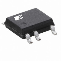
... Package Identifier D Plastic SO-8 • Package Material G GREEN: Halogen Free and RoHS Compliant • Tape & Reel and Other Options Blank Standard Configurations TL Tape & Reel, 2.5 k pcs. LNK632DG DETAIL 0.25 (0.010) 1.04 (0.041) REF BSC 0.40 (0.016) 1.27 (0.050) DETAIL ...
Page 10
... The products and applications illustrated herein (including transformer construction and circuits external to the products) may be covered by one or more U.S. and foreign patents, or potentially by pending U.S. and foreign patent applications assigned to Power Integrations. A complete list of Power Integrations patents may be found at www.powerint.com. Power Integrations grants its customers a license under certain patent rights as set forth at http://www ...