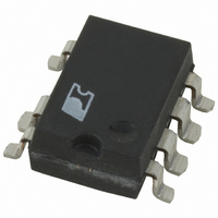
LNK520GN Power Integrations, LNK520GN Datasheet - Page 7

LNK520GN
Manufacturer Part Number
LNK520GN
Description
IC SWIT OCP CV/CC HV 8SMD
Manufacturer
Power Integrations
Series
LinkSwitch®r
Datasheet
1.LNK520PN.pdf
(20 pages)
Specifications of LNK520GN
Output Isolation
Isolated
Frequency Range
24 ~ 49.5kHz
Voltage - Output
700V
Power (watts)
5.50W
Operating Temperature
-40°C ~ 150°C
Package / Case
8-SMD Gull Wing, 7 Leads
Output Voltage
5.6 V
Input / Supply Voltage (max)
265 VAC
Input / Supply Voltage (min)
85 VAC
Duty Cycle (max)
80 %
Switching Frequency
42 KHz
Supply Current
0.75 mA
Operating Temperature Range
- 40 C to + 150 C
Mounting Style
SMD/SMT
For Use With
596-1006 - KIT DESIGN ACCELERATOR ADAPTER
Lead Free Status / RoHS Status
Lead free / RoHS Compliant
Available stocks
Company
Part Number
Manufacturer
Quantity
Price
Company:
Part Number:
LNK520GN
Manufacturer:
POWER
Quantity:
15 000
Part Number:
LNK520GN
Manufacturer:
POWER
Quantity:
20 000
Company:
Part Number:
LNK520GN-TL
Manufacturer:
ST
Quantity:
245
Company:
Part Number:
LNK520GN-TL
Manufacturer:
PowerInt
Quantity:
3 000
Part Number:
LNK520GN-TL
Manufacturer:
POWER
Quantity:
20 000
Figure 10. 2.75 W Constant Voltage/Constant Current (CV/CC) Charger Using LinkSwitch.
The secondary of the transformer is rectified and filtered by
D7 and C6 to provide the DC output to the load. LinkSwitch
dramatically simplifies the secondary side by controlling both
the constant voltage and constant current regions entirely from
the primary side. This is achieved by monitoring the primary-
side bias voltage.
85 - 265
VAC
N
L
Figure 11. Measured Output Characteristic of the Circuit in Figure 10.
8.2 Ω
RF1
2 W
10
9
8
7
6
5
4
3
2
1
0
0
1N4005
1N4005
D3
D1
1N4005
1N4005
D2
D4
100
4.7 µF
400 V
0.15 A
1 mH
C1
L1
4.7 µF
400 V
200
390 kΩ
C2
100 Ω
1/4 W
R1
R2
D
S
LinkSwitch
330 pF
C
1N4007GP
1 kV
Output Current (mA)
C4
LNK520P
D5
300
U1
220 nF
100T
C5
2
1
L
P
Diode D5, C4, R1 and R2 form the primary clamp network.
This limits the peak DRAIN voltage due to leakage inductance.
Resistor R2 allows the use of a slow, low cost rectifier diode
by limiting the reverse current through D5 when U1 turns on.
The selection of a slow diode improves radiated EMI and also
improves CV regulation, especially at no-load.
= 2.52 mH
EE16
T1
400
7
6
5
4
26T
8T
1%, 1/4 W
11DQ06
1N4937
6.81
D6B
D7
R4
kΩ
J1
500
15 Ω
R3
330 µF
16 V
C6
PI-3723-111303
600
1 µF
50 V
C3
5.5 V, 500 mA
85 VAC
115 VAC
190 VAC
230 VAC
265 VAC
Limits
RTN
LNK520
700
2/05
E
7


