PKS605YN Power Integrations, PKS605YN Datasheet - Page 6
PKS605YN
Manufacturer Part Number
PKS605YN
Description
IC OFFLINE SWIT OTP OCP HV TO220
Manufacturer
Power Integrations
Series
PeakSwitch®r
Specifications of PKS605YN
Mfg Application Notes
PeakSwitch Design Guide AppNote
Output Isolation
Isolated
Frequency Range
250 ~ 304kHz
Voltage - Output
700V
Power (watts)
79W
Operating Temperature
-40°C ~ 150°C
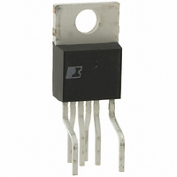
Package / Case
TO-220-7 (Formed Leads), 5 Leads
Output Voltage
24 V
Input / Supply Voltage (max)
265 VAC
Input / Supply Voltage (min)
85 VAC
Duty Cycle (max)
65 %
Switching Frequency
47 KHz
Supply Current
25 uA
Operating Temperature Range
- 40 C to + 150 C
Mounting Style
Through Hole
For Use With
596-1126 - KIT DESIGN ACC PEAKSWITCH FAMILY
Lead Free Status / RoHS Status
Lead free / RoHS Compliant
Other names
596-1121-5
Available stocks
Company
Part Number
Manufacturer
Quantity
Price
Company:

Part Number:
PKS605YN
Manufacturer:
POWER
Quantity:
15 000


of a PeakSwitch design are constant, the power delivered
to the load is proportional to the primary inductance of the
transformer and peak primary current squared. Hence, designing
the supply involves calculating the primary inductance of the
transformer for the maximum output power required. If the
chosen PeakSwitch family member is appropriate for the power
level, the current in the calculated inductance will ramp up to
current limit before the DC
Enable Function
PeakSwitch senses the EN/UV pin to determine whether or not
to proceed with the next switching cycle as described earlier.
The sequence of cycles is used to determine the current limit.
Once a cycle is started, it always completes the cycle (even when
the EN/UV pin changes state half way through the cycle). This
operation results in a power supply in which the output voltage
ripple is determined by the output capacitor, amount of energy
per switch cycle and the delay of the feedback.
The EN/UV pin signal is produced on the secondary by
comparing the power supply output voltage with a reference
voltage. The EN/UV pin signal is high when the power supply
output voltage is less than the reference voltage.
In a typical implementation, the EN/UV pin is driven by an
optocoupler. The collector of the optocoupler transistor is
connected to the EN/UV pin and the emitter is connected to
the SOURCE pin. The optocoupler LED is connected in series
with a Zener diode across the DC output voltage to be regulated.
When the output voltage exceeds the target regulation voltage
level (optocoupler LED voltage drop plus Zener voltage), the
optocoupler LED will start to conduct, pulling the EN/UV pin
Figure 9. PeakSwitch Operation at Medium Loading.
Rev. I 02/07
6
V
CLOCK
D
I
DRAIN
DRAIN
MAX
V
EN
PKS603-607
MAX
limit is reached.
PI-2377-091100
Figure 10. PeakSwitch Operation at Very Light Loading.
low. The Zener diode can be replaced by a TL431 reference
circuit for improved accuracy.
ON/OFF Operation with Current-Limit State Machine
The internal clock of the PeakSwitch runs all the time. At the
beginning of each clock cycle, it samples the EN/UV pin to
decide whether or not to implement a switch cycle, and based
on the sequence of samples over multiple cycles, it determines
the appropriate current limit. At high loads, when the EN/UV
pin is high (less than 240 µA out of the pin), a switching cycle
with the full current limit occurs. A t lighter loads, when EN/UV
is high, a switching cycle with a reduced current limit occurs.
200
100
300
200
100
Figure 11. PeakSwitch Power Up with Optional External UV
0
5
0
0
V
I
CLOCK
0
D
DRAIN
DRAIN
MAX
V
EN
V
V
V
DC-INPUT
DRAIN
BYPASS
Resistor (4 MW) Connected to EN/UV Pin.
Time (ms)
5
PI-2661-072400
10
Related parts for PKS605YN
Image
Part Number
Description
Manufacturer
Datasheet
Request
R

Part Number:
Description:
SOP-16
Manufacturer:
Power Integrations
Datasheet:
Part Number:
Description:
DIP8
Manufacturer:
Power Integrations
Datasheet:
Part Number:
Description:
TO-263
Manufacturer:
Power Integrations
Datasheet:
Part Number:
Description:
TO-263
Manufacturer:
Power Integrations
Datasheet:
Part Number:
Description:
Manufacturer:
Power Integrations
Datasheet: