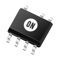
NCP1207BDR2G ON Semiconductor, NCP1207BDR2G Datasheet - Page 4

NCP1207BDR2G
Manufacturer Part Number
NCP1207BDR2G
Description
IC CTRLR PWM CM OVP OCP HV 8SOIC
Manufacturer
ON Semiconductor
Datasheet
1.NCP1207APG.pdf
(17 pages)
Specifications of NCP1207BDR2G
Output Isolation
Isolated
Voltage - Input
10.6 ~ 20 V
Operating Temperature
-40°C ~ 150°C
Package / Case
8-SOIC (0.154", 3.90mm Width) 7 leads
Number Of Outputs
1
Duty Cycle (max)
28.6 %
Output Current
500 mA
Mounting Style
SMD/SMT
Switching Frequency
75 KHz
Operating Supply Voltage
20 V
Maximum Operating Temperature
+ 150 C
Fall Time
20 ns
Minimum Operating Temperature
- 40 C
Rise Time
40 ns
Synchronous Pin
No
Topology
Flyback
Lead Free Status / RoHS Status
Lead free / RoHS Compliant
Available stocks
Company
Part Number
Manufacturer
Quantity
Price
Company:
Part Number:
NCP1207BDR2G
Manufacturer:
ON Semiconductor
Quantity:
1 950
Part Number:
NCP1207BDR2G
Manufacturer:
ON/安森美
Quantity:
20 000
1. Max value at T
ELECTRICAL CHARACTERISTICS
V
DYNAMIC SELF- -SUPPLY
INTERNAL STARTUP CURRENT SOURCE (T
DRIVE OUTPUT
CURRENT COMPARATOR (Pin 5 Unloaded)
OVERVOLTAGE SECTION (V
FEEDBACK SECTION (V
DEMAGNETIZATION DETECTION BLOCK
CC
V
V
V
V
Internal IC Consumption, No Output Load on Pin 5,
Internal IC Consumption, 1.0 nF Output Load on Pin 5,
Internal IC Consumption in Latchoff Phase
High--voltage Current Source, V
High--voltage Current Source, V
Output Voltage Rise--time @ CL = 1.0 nF, 10--90% of Output Signal
Output Voltage Fall--time @ CL = 1.0 nF, 10--90% of Output Signal
Source Resistance
Sink Resistance
Input Bias Current @ 1.0 V Input Level on Pin 3
Maximum Internal Current Setpoint
Propagation Delay from Current Detection to Gate OFF State
Leading Edge Blanking Duration
Internal Current Offset Injected on the CS Pin during OFF Time
Sampling Delay after ON Time
OVP Internal Reference Level
Internal Pull--up Resistor
Pin 3 to Current Setpoint Division Ratio
Internal Soft--start
Input Threshold Voltage (Vpin 1 Decreasing)
Hysteresis (Vpin 1 Decreasing)
Input Clamp Voltage
Demag Propagation Delay
Internal Input Capacitance at Vpin 1 = 1.0 V
Minimum T
Timeout After Last Demag Transition
Pin 1 Internal Impedance
CC
CC
CC
CC
F
F
= 11 V unless otherwise noted)
SW
SW
Increasing Level at which the Current Source Turns--off
Decreasing Level at which the Current Source Turns--on
Decreasing Level at which the Latchoff Phase Ends
Level at which Output Pulses are Disabled
= 60 kHz
= 60 kHz
OFF
(Internal Blanking Delay after T
J
= 0C.
CC
= 11 V, Pin 5 Loaded by 1.0 kΩ)
CC
Rating
CC
CC
= 11 V)
= 10 V
= 0
High State (Ipin 1 = 3.0 mA)
Low State (Ipin 1 = --2.0 mA)
(For typical values T
J
ON
> 0C)
)
http://onsemi.com
NCP1207A
NCP1207B
NCP1207A
NCP1207B
J
= 25C, for min/max values T
4
Pin
6
6
6
6
6
6
6
8
8
5
5
5
5
3
3
3
3
3
1
1
2
1
1
1
1
1
1
1
1
1
--
--
VCC
VCC
Symbol
VCC
T
UVLO
T
ICC1
ICC2
ICC3
T
Iratio
T
T
Iskip
sample
R
I
VC
C
R
Rup
VC
V
T
R
IC1
IC2
Limit
Tss
V
blank
V
I
DEL
dem
T
T
LEB
out
OH
IB
par
OL
ref
int
th
H
r
OFF
latch
f
H
ON
L
J
= 0C to +125C, Max T
10.8
0.92
--0.9
Min
9.1
4.3
5.0
6.4
8.0
3.5
12
35
--
--
--
--
--
--
--
--
--
--
--
--
--
--
--
--
--
--
--
--
--
--
--200mV
VCC
0.02
--0.7
Typ
330
100
380
200
210
5.3
1.0
1.6
7.0
8.0
1.0
4.5
1.5
7.2
3.3
1.0
8.0
4.5
5.0
12
10
40
20
20
10
20
50
20
10
10
28
ON
J
= 150C,
(Note 1)
(Note 1)
Max
12.9
10.6
1.12
--0.5
160
1.3
2.0
9.6
8.0
5.5
36
19
90
12
--
--
--
--
--
--
--
--
--
--
--
--
--
--
--
--
--
--
--
Unit
mA
mA
mA
mA
mV
mV
kΩ
ms
kΩ
mA
mA
mA
pF
ns
ns
ns
ns
ms
ns
ms
ms
V
V
V
V
Ω
Ω
V
V
V
V
--


