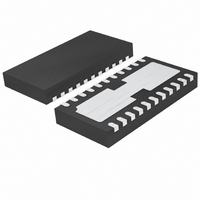
LTC4090EDJC#PBF Linear Technology, LTC4090EDJC#PBF Datasheet - Page 22

LTC4090EDJC#PBF
Manufacturer Part Number
LTC4090EDJC#PBF
Description
IC USB POWER MANAGER 22-DFN
Manufacturer
Linear Technology
Datasheet
1.LTC4090EDJCPBF.pdf
(28 pages)
Specifications of LTC4090EDJC#PBF
Function
Power Management
Battery Type
Lithium-Ion (Li-Ion), Lithium-Polymer (Li-Pol)
Voltage - Supply
4.35 V ~ 5.5 V
Operating Temperature
-40°C ~ 85°C
Mounting Type
Surface Mount
Package / Case
22-WFDFN Exposed Pad
Supply Voltage Range
4.35V To 5.5V
Operating Temperature Range
-40°C To +85°C
Digital Ic Case Style
DFN
No. Of Pins
22
Msl
MSL 1 - Unlimited
Termination Type
SMD
Supply Voltage Min
4.35V
Rohs Compliant
Yes
Filter Terminals
SMD
Frequency
2.7MHz
Lead Free Status / RoHS Status
Lead free / RoHS Compliant
Available stocks
Company
Part Number
Manufacturer
Quantity
Price
LTC4090/LTC4090-5
APPLICATIONS INFORMATION
If low quiescent current is not required, the LTC4090/
LTC4090-5 can operate in pulse-skipping mode. The benefi t
of this mode is that the LTC4090/LTC4090-5 will enter full
frequency standard PWM operation at a lower output load
current than when in Burst Mode operation. The front page
application circuit will switch at full frequency at output
loads higher than about 60mA.
Boost Pin Considerations
Capacitor C2 (see Block Diagram) and an internal diode
are used to generate a boost voltage that is higher than
the input voltage. In most cases, a 0.47μF capacitor will
work well. The BOOST pin must be at least 2.3V above
the SW pin for proper operation.
High Voltage Regulator Soft-Start
The HVEN pin can be used to soft-start the high voltage
regulator of the LTC4090/LTC4090-5, reducing maximum
input current during start-up. The HVEN pin is driven
through an external RC fi lter to create a voltage ramp at
this pin. Figure 7 shows the start-up and shutdown wave-
forms with the soft-start circuit. By choosing a large RC
time constant, the peak start-up current can be reduced
to the current that is required to regulate the output, with
no overshoot. Choose the value of the resistor so that it
can supply 20μA when the HVEN pin reaches 2.3V.
Synchronization and Mode
The SYNC pin allows the high voltage regulator to be
synchronized to an external clock.
22
RUN
15k
0.22μF
Figure 7. To Soft-Start the High Voltage Regulator,
Add a Resistor and Capacitor to the HVEN Pin
HVEN
GND
2ms/DIV
4090 F07
I
1A/DIV
HVEN
2V/DIV
V
2V/DIV
L
OUT
Synchronizing the LTC4090/LTC4090-5 internal oscillator
to an external frequency can be done by connecting a
square wave (with 20% to 80% duty cycle) to the SYNC
pin. The square wave amplitude should be such that the
valleys are below 0.3V and the peaks are above 0.8V (up
to 6V). The high voltage regulator may be synchronized
over a 300kHz to 2MHz range. The R
chosen such that the LTC4090/LTC4090-5 oscillate 25%
lower than the external synchronization frequency to ensure
adequate slope compensation. While synchronized, the
high voltage regulator will turn on the power switch on
positive going edges of the clock. When the power good
(PG) output is low, such as during start-up, short-circuit,
and overload conditions, the LTC4090/LTC4090-5 will dis-
able the synchronization feature. The SYNC pin should be
grounded when synchronization is not required.
Alternate NTC Thermistors and Biasing
The LTC4090/LTC4090-5 provide temperature qualifi ed
charging if a grounded thermistor and a bias resistor are
connected to NTC (see Figure 8). By using a bias resistor
whose value is equal to the room temperature resistance
of the thermistor (R
are preprogrammed to approximately 50°C and 0°C, re-
spectively (assuming a Vishay curve 2 thermistor).
The upper and lower temperature thresholds can be ad-
justed by either a modifi cation of the bias resistor value
or by adding a second adjustment resistor to the circuit.
If only the bias resistor is adjusted, then either the upper
or the lower threshold can be modifi ed but not both. The
other trip point will be determined by the characteristics
of the thermistor. Using the bias resistor in addition to an
adjustment resistor, both the upper and the lower tempera-
ture trip points can be independently programmed with
the constraint that the difference between the upper and
lower temperature thresholds cannot decrease. Examples
of each technique are given below.
NTC thermistors have temperature characteristics which
are indicated on resistance-temperature conversion tables.
The Vishay-Dale thermistor NTHS0603N02N1002J, used
in the following examples, has a nominal value of 10k
and follows the Vishay curve 2 resistance-temperature
characteristic. The LTC4090/LTC4090-5’s trip points are
25C
) the upper and lower temperatures
T
resistor should be
4090fc


