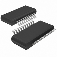
LTC4008EGN-1#PBF Linear Technology, LTC4008EGN-1#PBF Datasheet - Page 16

LTC4008EGN-1#PBF
Manufacturer Part Number
LTC4008EGN-1#PBF
Description
IC BATT CHARGER CTRLR 4A 20SSOP
Manufacturer
Linear Technology
Datasheet
1.LTC4008EGNPBF.pdf
(24 pages)
Specifications of LTC4008EGN-1#PBF
Function
Charge Management
Battery Type
Multi-Chemistry
Voltage - Supply
6 V ~ 28 V
Operating Temperature
-40°C ~ 85°C
Mounting Type
Surface Mount
Package / Case
20-SSOP (0.200", 5.30mm Width)
Lead Free Status / RoHS Status
Lead free / RoHS Compliant
Available stocks
Company
Part Number
Manufacturer
Quantity
Price
LTC4008
APPLICATIONS INFORMATION
Selection criteria for the power MOSFETs include the “ON”
resistance R
transfer capacitance C
output current. The charger is operating in continuous
mode so the duty cycles for the top and bottom MOSFETs
are given by:
The MOSFET power dissipations at maximum output
current are given by:
Where δΔT is the temperature dependency of R
k is a constant inversely related to the gate drive current.
Both MOSFETs have I
includes an additional term for transition losses, which
are highest at high input voltages. For V
current effi ciency generally improves with larger MOSFETs,
while for V
the point that the use of a higher R
C
MOSFET losses are greatest at high input voltage or during
a short circuit when the duty cycle in this switch in nearly
100%. The term (1 + δΔT) is generally given for a MOSFET
in the form of a normalized R
but δ = 0.005/°C can be used as an approximation for low
voltage MOSFETs. C
in the MOSFET characteristics. The constant k = 2 can be
used to estimate the contributions of the two terms in the
main switch dissipation equation.
If the charger is to operate in low dropout mode or with
a high duty cycle greater than 85%, then the topside P-
channel effi ciency generally improves with a larger MOSFET.
Using asymmetrical MOSFETs may achieve cost savings
or effi ciency gains.
16
RSS
Main Switch Duty Cycle = V
Synchronous Switch Duty Cycle = (V
PMAIN = V
+ k(V
PSYNC = (V
actually provides higher effi ciency. The synchronous
IN
)
IN
2
(I
> 20V the transition losses rapidly increase to
DS(ON)
MAX
OUT
IN
)(C
– V
/V
, total gate capacitance Q
IN(IMAX)
RSS
RSS
OUT
2
R losses while the PMAIN equation
RSS
)(f
)/V
= Q
OSC
, input voltage and maximum
2
IN
(1 + δΔT)R
GD
DS(ON)
(I
)
OUT
MAX
/ΔV
DS(ON)
/V
DS
)
vs temperature curve,
2
IN
(1 + δΔT)R
is usually specifi ed
DS(ON)
device with lower
IN
IN
< 20V the high
– V
OUT
G
DS(ON)
, reverse
DS(ON)
)/V
IN
and
.
The Schottky diode D1, shown in the Typical Application
on the back page, conducts during the dead-time between
the conduction of the two power MOSFETs. This prevents
the body diode of the bottom MOSFET from turning on and
storing charge during the dead-time, which could cost as
much as 1% in effi ciency. A 1A Schottky is generally a good
size for 4A regulators due to the relatively small average
current. Larger diodes can result in additional transition
losses due to their larger junction capacitance.
The diode may be omitted if the effi ciency loss can be
tolerated.
Calculating IC Power Dissipation
The power dissipation of the LTC4008 is dependent upon
the gate charge of the top and bottom MOSFETs (Q
Q
manufacturer’s data sheet and is dependent upon both
the gate voltage swing and the drain voltage swing of the
MOSFET. Use 6V for the gate voltage swing and V
the drain voltage swing.
Example:
Adapter Limiting
An important feature of the LTC4008 is the ability to auto-
matically adjust charging current to a level which avoids
overloading the wall adapter. This allows the product to
operate at the same time that batteries are being charged
without complex load management algorithms. Addition-
ally, batteries will automatically be charged at the maximum
possible rate of which the adapter is capable.
This feature is created by sensing total adapter output cur-
rent and adjusting charging current downward if a preset
adapter current limit is exceeded. True analog control is
G2
PD = V
V
I
PD = 292mW
Q
DCIN
respectively) The gate charge is determined from the
= 5mA
= 19V, f
DCIN
• (f
OSC
OSC
= 345kHz, Q
(Q
G1
+ Q
G2
) + I
G1
= Q
Q
)
G2
= 15nC,
DCIN
G1
4008fb
for
&


