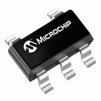
MCP73831T-2ATI/OT Microchip Technology, MCP73831T-2ATI/OT Datasheet - Page 18

MCP73831T-2ATI/OT
Manufacturer Part Number
MCP73831T-2ATI/OT
Description
IC CONTROLLR LI-ION 4.2V SOT23-5
Manufacturer
Microchip Technology
Datasheet
1.MCP73831T-2DCIOT.pdf
(28 pages)
Specifications of MCP73831T-2ATI/OT
Battery Type
Lithium-Ion (Li-Ion), Lithium-Polymer (Li-Pol)
Function
Charge Management
Voltage - Supply
3.75 V ~ 6 V
Operating Temperature
-40°C ~ 85°C
Mounting Type
Surface Mount
Package / Case
SC-74A, SOT-753
Input Voltage
6V
Battery Charge Voltage
4.2V
Charge Current Max
500mA
Battery Ic Case Style
SOT-23
No. Of Pins
5
No. Of Series Cells
1
Output Voltage
4.2 V
Operating Supply Voltage
3.75 V to 6 V
Maximum Operating Temperature
+ 85 C
Minimum Operating Temperature
- 40 C
Mounting Style
SMD/SMT
Lead Free Status / RoHS Status
Contains lead / RoHS non-compliant
Lead Free Status / RoHS Status
Lead free / RoHS Compliant, Contains lead / RoHS non-compliant
Other names
MCP73831T-2ATI/OT
MCP73831T-2ATI/OTTR
MCP73831T-2ATI/OTTR
Available stocks
Company
Part Number
Manufacturer
Quantity
Price
Company:
Part Number:
MCP73831T-2ATI/OT
Manufacturer:
BOURNS
Quantity:
33 000
Part Number:
MCP73831T-2ATI/OT
Manufacturer:
MICROCHIP/微芯
Quantity:
20 000
MCP73831/2
6.1.1.2
The worst-case power dissipation in the battery
charger occurs when the input voltage is at the
maximum and the device has transitioned from the
Preconditioning mode to the Constant-Current mode.
In this case, the power dissipation is:
Power dissipation with a 5V, ±10% input voltage source
is:
This power dissipation with the battery charger in the
SOT-23-5 package will cause thermal regulation to be
entered as depicted in
2mm x 3mm DFN package could be utilized to reduce
charge cycle times.
6.1.1.3
The MCP73831/2 are stable with or without a battery
load. In order to maintain good AC stability in the Con-
stant-Voltage mode, a minimum capacitance of 4.7 µF
is recommended to bypass the V
capacitance provides compensation when there is no
battery load. In addition, the battery and interconnec-
tions appear inductive at high frequencies. These
elements are in the control feedback loop during
Constant-Voltage mode. Therefore, the bypass capac-
itance may be necessary to compensate for the
inductive nature of the battery pack.
Virtually any good quality output filter capacitor can be
used, independent of the capacitor’s minimum
Effective Series Resistance (ESR) value. The actual
value of the capacitor (and its associated ESR)
depends on the output load current. A 4.7 µF ceramic,
tantalum or aluminum electrolytic capacitor at the
output is usually sufficient to ensure stability for output
currents up to a 500 mA.
6.1.1.4
The MCP73831/2 provide protection from a faulted or
shorted input. Without the protection, a faulted or
shorted input would discharge the battery pack through
the body diode of the internal pass transistor.
DS21984E-page 18
Where:
PowerDissipation
I
V
PowerDissipation
V
REGMAX
PTHMIN
DDMAX
Thermal Considerations
External Capacitors
Reverse-Blocking Protection
= the maximum input voltage
= the maximum fast charge current
= the minimum transition threshold
voltage
=
(
=
V
DDMAX
(
5.5V 2.7V
Figure
–
–
V
6-3. Alternatively, the
PTHMIN
) 550mA
BAT
×
pin to V
)
×
I
REGMAX
=
1.54W
SS
. This
6.1.1.5
The current regulation set input pin (PROG) can be
used to terminate a charge at any time during the
charge cycle, as well as to initiate a charge cycle or
initiate a recharge cycle.
Placing a programming resistor from the PROG input to
V
float or by applying a logic-high input signal, disables
the device and terminates a charge cycle. When
disabled, the device’s supply current is reduced to
25 µA, typically.
6.1.1.6
A status output provides information on the state of
charge. The output can be used to illuminate external
LEDs or interface to a host microcontroller. Refer to
Table 5-1
output during a charge cycle.
6.2
For optimum voltage regulation, place the battery pack
as close as possible to the device’s V
This is recommended to minimize voltage drops along
the high current-carrying PCB traces.
If the PCB layout is used as a heatsink, adding many
vias in the heatsink pad can help conduct more heat to
the backplane of the PCB, thus reducing the maximum
junction temperature.
typical layout with PCB heatsinking.
FIGURE 6-4:
FIGURE 6-5:
SS
enables the device. Allowing the PROG input to
PCB Layout Issues
for a summary of the state of the status
Charge Inhibit
Charge Status Interface
Typical Layout (Top).
Typical Layout (Bottom).
Figures 6-4
© 2008 Microchip Technology Inc.
and
BAT
and V
6-5
depict a
SS
pins.


