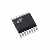
LTC1730EGN-4 Linear Technology, LTC1730EGN-4 Datasheet - Page 5

LTC1730EGN-4
Manufacturer Part Number
LTC1730EGN-4
Description
IC BATT PULSE CHRGR LI-ION16SSOP
Manufacturer
Linear Technology
Datasheet
1.LTC1730ES8-4.2PBF.pdf
(12 pages)
Specifications of LTC1730EGN-4
Function
Charge Management
Battery Type
Lithium-Ion (Li-Ion)
Voltage - Supply
4.5 V ~ 12 V
Operating Temperature
-40°C ~ 85°C
Mounting Type
Surface Mount
Package / Case
16-SSOP (0.150", 3.90mm Width)
Lead Free Status / RoHS Status
Contains lead / RoHS non-compliant
Available stocks
Company
Part Number
Manufacturer
Quantity
Price
Company:
Part Number:
LTC1730EGN-4
Manufacturer:
LT
Quantity:
10 000
Part Number:
LTC1730EGN-4
Manufacturer:
LINEAR/凌特
Quantity:
20 000
LTC1730ES8-4.2
SENSE (Pin 1): Maximum Overcurrent Sense Input. A
sense resistor (R
the SENSE pin. When the voltage drop across R
exceeds 100mV, the pass transistor immediately turns off
and turns back on after a 400ms time-out period (C
= 0.1 F). The on-off cycle will continue, as long as the
overcurrent condition persists or until the timer runs out.
If overcurrent protection is not needed, short SENSE to
V
V
13.2V). Bypass this pin with a 1 F capacitor in series with
a 4.7 resistor. An RC network from the V
GATE pin is also required. The capacitor controls the slew
rate at the V
current when the input voltage is first applied. When the
pass transistor turns on, V
manner, with a slope equal to 10 A/C. When the pass
transistor turns off, V
CHRG (Pin 3): Open-Drain Charge Status Output. When a
depleted battery is being charged, the CHRG pin is pulled
to ground by an N-MOSFET capable of driving an LED.
Once the duty cycle at the GATE pin drops below 10%, the
N-MOSFET turns off and a weak 40 A current source to
ground turns on to indicate a near end-of-charge (C/10)
condition. When a time-out occurs or the input supply is
removed, the CHRG pin goes high impedance.
GND (Pin 4): Electrical Ground Connection and provides
a thermal path from the IC to the PC board copper. Use
large copper pads and traces for maximum heat transfer.
TIMER (Pin 5): Timer Set Pin. The timer period is set by a
capacitor (C
t
OFF time and the overcurrent time-out period are all set by
the same timer period.
NTC/SHDN (Pin 6): Input to the NTC (Negative Tempera-
ture Coefficient) Thermistor Monitoring and Shutdown
Circuitry. With an external 10k NTC thermistor to ground
and a 1% resistor to V
ture of the battery pack and stop charging when the
temperature is out of range. When the voltage at this pin
drops below 0.5 • V
PI FU CTIO S
TIMER
CC
CC
U
.
(Pin 2): Positive Input Supply Voltage (4.5V V
= (C
U
TIMER
CC
TIMER
pin, while the resistor limits the inrush
SENSE
• 3Hr)/(0.1 F). The minimum ON time,
) to ground. The timer period is:
CC
U
CC
CC
, or 2V at hot temperature or rises
) should be connected from V
ramps up with a slope of 40 A/C.
, this pin can sense the tempera-
CC
ramps down in a controlled
CC
pin to the
SENSE
TIMER
CC
CC
to
above 0.875 • V
charge cycle is suspended and the internal timer is frozen.
The CHRG pin output status is not affected in this hold
state.
When this pin is pulled below 50mV, the IC goes into the
shutdown mode. The charging stops (the GATE pin is
pulled to ground) the timer is reset and the CHRG pin goes
into a high impedance state.
GATE (Pin 7): Gate Drive Output Pin for Internal and
External Pass Transistors. An external N-MOSFET transis-
tor can be connected in parallel with the internal transistor
to reduce the on-resistance for higher charge current. In
this case, an external blocking diode is required to prevent
damage to the battery if V
current source pulls this pin up to the charge pump
potential when turned on and a 40 A current source pulls
it down to ground to turn it off. If an overcurrent condition
is detected, the GATE pin is immediately pulled to ground.
A series RC network from the GATE to the V
required to control the slew rate at the V
switch is turned on or off. The slew rate control prevents
excessive current from the capacitor located in the wall
adapter from flowing into the battery when the pass
transistor is turned on. The voltage at this pin is internally
clamped to 12V above the BAT pin.
BAT (Pin 8): Battery Sense Input Pin. This pin is clamped
to 4.7V if the battery is disconnected while charging. An
internal resistor divider presets the final float voltage to
4.2V.
If the voltage at the BAT pin drops 150mV below final float
voltage after the charge cycle has ended, the timer resets
and a new charge cycle begins.
LTC1730EGN-4
GND (Pins 1, 8, 9, 16): Refer to LTC1730ES8-4.2
SENSE (Pin 2): Refer to LTC1730ES8-4.2
V
ACPR (Pin 4): Wall Adapter Present Open-Drain Output.
When the input voltage (wall adapter) is applied to the
LTC1730, this pin is pulled to ground by an internal
CC
(Pin 3): Refer to LTC1730ES8-4.2
LTC1730-4/LTC1730-4.2
CC
, or 3.5V at cold (with V
CC
is shorted to ground. A 10 A
CC
CC
pin when the
= 4V), the
CC
sn1730 1730fs
pin is
5


