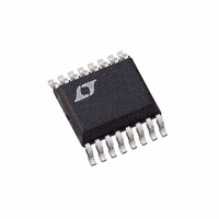
LTC4006EGN-2#TR Linear Technology, LTC4006EGN-2#TR Datasheet - Page 14

LTC4006EGN-2#TR
Manufacturer Part Number
LTC4006EGN-2#TR
Description
IC CHARGER BATTERY 4A 16-SSOP
Manufacturer
Linear Technology
Datasheet
1.LTC4006EGN-2PBF.pdf
(20 pages)
Specifications of LTC4006EGN-2#TR
Function
Charge Management
Battery Type
Lithium-Ion (Li-Ion)
Voltage - Supply
6 V ~ 28 V
Operating Temperature
-40°C ~ 85°C
Mounting Type
Surface Mount
Package / Case
16-SSOP (0.150", 3.90mm Width)
Output Current
4A
Output Voltage
12.6V
Operating Supply Voltage (min)
6V
Operating Supply Voltage (max)
28V
Operating Temp Range
-40C to 85C
Package Type
SSOP N
Mounting
Surface Mount
Pin Count
16
Operating Temperature Classification
Industrial
Lead Free Status / RoHS Status
Contains lead / RoHS non-compliant
Lead Free Status / RoHS Status
Contains lead / RoHS non-compliant
Available stocks
Company
Part Number
Manufacturer
Quantity
Price
APPLICATIO S I FOR ATIO
LTC4006
Table 4
Charger Switching Power MOSFET
and Diode Selection
Two external power MOSFETs must be selected for use
with the charger: a P-channel MOSFET for the top (main)
switch and an N-channel MOSFET for the bottom (syn-
chronous) switch.
The peak-to-peak gate drive levels are set internally. This
voltage is typically 6V. Consequently, logic-level threshold
MOSFETs must be used. Pay close attention to the BV
specification for the MOSFETs as well; many of the logic
level MOSFETs are limited to 30V or less.
Selection criteria for the power MOSFETs include the “ON”
resistance R
transfer capacitance C
output current. The charger is operating in continuous
mode at moderate to high currents so the duty cycles for
the top and bottom MOSFETs are given by:
The MOSFET power dissipations at maximum output
current are given by:
Where δ is the temperature dependency of R
is a constant inversely related to the gate drive current.
Both MOSFETs have I
includes an additional term for transition losses, which are
14
AVERAGE CURRENT (A)
Main Switch Duty Cycle = V
Synchronous Switch Duty Cycle = (V
PMAIN = V
PSYNC = (V
MAXIMUM
1
1
2
2
3
3
4
4
+ k(V
DS(ON)
OUT
IN
– V
/V
2
, total gate capacitance Q
IN
U
IN
)(I
OUT
2
(I
R losses while the PMAIN equation
RSS
VOLTAGE (V)
2
MAX
)/V
MAX
U
INPUT
, input voltage and maximum
≤ 20
> 20
≤ 20
> 20
≤ 20
> 20
≤ 20
> 20
)(C
IN
)(1 + δ∆T)R
(I
RSS
OUT
2
MAX
)(f
/V
W
)(1 + δ∆T)R
IN
OSC
MINIMUM INDUCTOR
IN
)
DS(ON)
VALUE (µH)
40 ±20%
56 ±20%
20 ±20%
30 ±20%
15 ±20%
20 ±20%
10 ±20%
15 ±20%
– V
DS(ON)
OUT
G
U
, reverse
DS(ON)
)/V
and k
IN
DSS
.
highest at high input voltages. For V
current efficiency generally improves with larger MOSFETs,
while for V
to the point that the use of a higher R
lower C
chronous MOSFET losses are greatest at high input volt-
age or during a short circuit when the duty cycle in this
switch is nearly 100%. The term (1 + δ∆T) is generally
given for a MOSFET in the form of a normalized R
temperature curve, but δ = 0.005/°C can be used as an
approximation for low voltage MOSFETs. C
specified in the MOSFET characteristics; if not, then C
can be calculated using C
k = 2 can be used to estimate the contributions of the two
terms in the main switch dissipation equation.
If the charger is to operate in low dropout mode or with a
high duty cycle greater than 85%, then the topside
P-channel efficiency generally improves with a larger
MOSFET. Using asymmetrical MOSFETs may achieve cost
savings or efficiency gains.
The Schottky diode D1, shown in the Typical Application
on the back page, conducts during the dead-time between
the conduction of the two power MOSFETs. This prevents
the body diode of the bottom MOSFET from turning on and
storing charge during the dead-time, which could cost as
much as 1% in efficiency. A 1A Schottky is generally a
good size for 4A regulators due to the relatively small
average current. Larger diodes can result in additional
transition losses due to their larger junction capacitance.
The diode may be omitted if the efficiency loss can be
tolerated.
Calculating IC Power Dissipation
The power dissipation of the LTC4006 is dependent upon
the gate charge of the top and bottom MOSFETs (Q
Q
manufacturer’s data sheet and is dependent upon both the
gate voltage swing and the drain voltage swing of the
MOSFET. Use 6V for the gate voltage swing and V
the drain voltage swing.
G2
P
D
respectively). The gate charge is determined from the
= V
RSS
DCIN
IN
actually provides higher efficiency. The syn-
> 20V the transition losses rapidly increase
• (f
OSC
(Q
G1
RSS
+ Q
= Q
G2
) + I
GD
/∆V
DCIN
IN
DS(ON)
DS
)
< 20V the high
. The constant
RSS
device with
is usually
DS(ON)
DCIN
G1
4006fa
and
RSS
for
vs


