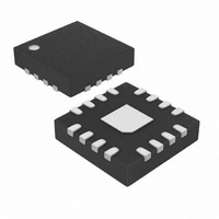
MAX8568AETE+ Maxim Integrated Products, MAX8568AETE+ Datasheet - Page 13

MAX8568AETE+
Manufacturer Part Number
MAX8568AETE+
Description
IC BATT MANAGE LITH 16-TQFN
Manufacturer
Maxim Integrated Products
Datasheet
1.MAX8568AETET.pdf
(17 pages)
Specifications of MAX8568AETE+
Function
Back-Up Management
Battery Type
Lithium-Ion (Li-Ion); Nickel-Metal Hydride (NiMH)
Voltage - Supply
2.8 V ~ 5.5 V
Operating Temperature
-40°C ~ 85°C
Mounting Type
Surface Mount
Package / Case
16-TQFN Exposed Pad
Lead Free Status / RoHS Status
Lead free / RoHS Compliant
The control scheme of the MAX8568 permits flexibility in
choosing an inductor. A 10µH inductor performs well in
most applications. Smaller inductance values typically
offer smaller physical size for a given series resistance,
allowing the smallest overall circuit dimensions. Circuits
using larger inductance may provide higher efficiency
and exhibit less ripple, but also may reduce the maxi-
mum output current. This occurs when the inductance is
sufficiently large to prevent the LX current limit (I
from being reached before the maximum on-time
(t
For maximum output current, choose the inductor value
so that the controller reaches the current limit before
the maximum on-time is reached:
where t
is typically 500mA (see the Electrical Characteristics
table).
For larger inductor values, determine the peak inductor
current (I
The output voltage is set to 2.5V or 3.3V, or is
adjustable. Connect BKV to GND for 3.3V, and BKV to
BKSU for 2.5V. The adjustable output voltage is set
from 2.5V to 5V using external resistors R1 and R2
(Figure 7). Since FB leakage is 50nA (max), select
feedback resistor R2 in the 100kΩ to 1MΩ range.
Calculate R1 as follows:
where V
The LDO output voltage is preset to 2.5V for the
MAX8568A and 1.8V for the MAX8568B. The LDO can
supply up to 10mA. The LDO output voltage is not
adjustable.
ON(MAX)
ON(MAX)
BKV
PEAK
) expires.
= 1.21V.
) by:
is typically 5µs, and the current limit (I
I
PEAK
R
L
______________________________________________________________________________________
1
<
=
=
V
R
BK
2
V
BK
Setting the Output Voltage
×
V
I
LIM
V
t
BKSU
ON MAX
×
BKV
Complete Backup-Management ICs
t
ON MAX
L
(
(
Inductor Selection
−
)
1
)
for Lithium and NiMH Batteries
LDO
LIM
LIM
)
)
Capacitors are required at the LDO output of the
MAX8568 for stable operation over the full load and tem-
perature range. A 4.7µF or greater X5R or X7R ceramic
capacitor is recommended. To reduce noise and
improve load-transient response, larger output capaci-
tors up to 10µF can be used. Surface-mount ceramic
capacitors have very low ESR and are commonly avail-
able in values up to 10µF. Note that some ceramic
dielectrics, such as Z5U and Y5V, exhibit large capaci-
tance and ESR variation with temperature and require
larger than the recommended values to maintain stability
and good load-transient response over temperature.
OD1 and OD2 are open-drain outputs and are
designed to be connected to the gates of external p-
channel MOSFETs (see Figure 7). These MOSFETs
connect the main system power supplies (I/O IN and
MEM IN) to the system loads (I/O OUT and MEM OUT)
during normal operation. During backup, they discon-
nect the power supplies from the system loads to pre-
vent the power supplies from drawing backup current
away from the system. For this reason, the MOSFETs
are connected “backwards” from what might be
expected. The source of the MOSFETs are connected
to the system load side (I/O OUT and MEM OUT). The
MOSFETs’ purpose is to block current flow from the
backup supply (BKSU) to the main supplies (I/O IN and
MEM IN). They do not block current flow from I/O IN to
I/O OUT and from MEM IN to MEM OUT. Even when off,
the MOSFET body diodes allow current to pass in that
direction.
OD1 is intended to drive the MOSFET switch for I/O IN
and I/O OUT, while OD2 is intended to drive the MOSFET
switch for MEM IN and MEM OUT. See the Typical
Operating Characteristics and Figure 1 for typical opera-
tion of OD1 and OD2.
The external MOSFET should be chosen based upon
R
(main battery > 2.8V), the current required for normal
operation of I/O and MEM goes through these external
MOSFETs. Choose an R
MOSFET voltage drop. When V
MOSFET turns off, and MEM and I/O are powered by
the MAX8568. The gate capacitance of the external
MOSFET must discharge through the external gate-to-
source resistor. This discharge time determines how
quickly the main supply is disconnected and isolated.
DS(ON)
External MOSFET Drivers—OD1, OD2
and gate capacitance. When V
External MOSFET Selection
DS(ON)
LDO Capacitor Selection
that minimizes the
INOK
INOK
< 2.43V, the
> 2.43V
13


