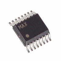
MAX1873SEEE+ Maxim Integrated Products, MAX1873SEEE+ Datasheet - Page 12

MAX1873SEEE+
Manufacturer Part Number
MAX1873SEEE+
Description
IC CNTRLR CHARGE LI+ 16-QSOP
Manufacturer
Maxim Integrated Products
Datasheet
1.MAX1873TEEET.pdf
(14 pages)
Specifications of MAX1873SEEE+
Function
Charge Management
Battery Type
Li-Ion, NiCd, NiMH
Voltage - Supply
6 V ~ 28 V
Operating Temperature
-40°C ~ 85°C
Mounting Type
Surface Mount
Package / Case
16-SSOP (0.150", 3.90mm Width)
Product
Charge Management
Operating Supply Voltage
6 V to 28 V
Supply Current
4 mA
Maximum Operating Temperature
+ 85 C
Minimum Operating Temperature
- 40 C
Charge Safety Timers
No
Mounting Style
SMD/SMT
Temperature Monitoring
No
Uvlo Start Threshold
0.05 V
Uvlo Stop Threshold
0.38 V
Lead Free Status / RoHS Status
Lead free / RoHS Compliant
For example, for a 4-cell charging current of 3A, a
V
be 11.2µH with a peak current of 3.75A. Therefore a
10µH inductor would be satisfactory.
The MAX1873 uses a P-channel power MOSFET
switch. The MOSFET must be selected to meet the effi-
ciency or power dissipation requirements of the charg-
ing circuit as well as the maximum temperature of the
MOSFET. Characteristics that affect MOSFET power
dissipation are drain-source on-resistance (
and gate charge. Generally these are inversely propor-
tional.
To determine MOSFET power dissipation, the operating
duty cycle must first be calculated. When the charger is
operating at higher currents, the inductor current will be
continuous (the inductor current will not drop to 0). In
this case, the high-side MOSFET duty cycle (D) can be
approximated by the equation:
And the catch-diode duty cycle (D') will be 1 - D or:
where V
4.2V per cell) and V
For MOSFETs, the worst-case power dissipation due to
on-resistance (P
where the operating conditions are minimum source-
voltage and maximum battery voltage. P
approximated by the equation:
Transition losses (P
equation:
where t
switching frequency. The total power dissipation of the
MOSFET is then:
Simple Current-Limited Switch-Mode
Li+ Charger Controller
12
DCIN(MAX)
______________________________________________________________________________________
TR
BATT
is the MOSFET transition time and f
P
R
of 24V, and an LIR of 0.5, L is calculated to
P
is the battery-regulation voltage (typically
=
T
I
PEAK
V
V
R
=
BATT MAX
DCIN MIN
D
) occurs at the maximum duty cycle,
V
DCIN
'≈
DCIN
=
T
D
(
V
(
) can be approximated by the
I
DCIN
CHG
≈
is the source-input voltage.
×
V
V
V
)
)
I
BATT
DCIN
CHG
DCIN
(
×
1
−
R
+
V
3
DS ON
LIR
BATT
MOSFET Selection
×
(
f
SW
2 /
)
)
×
×
I
CHG
t
TR
2
R
RDS(ON)
SW
can be
is the
)
A Schottky rectifier with a current rating of at least the
charge current limit must be connected from the MOS-
FET drain to GND. The voltage rating of the diode must
exceed the maximum expected input voltage.
The input capacitor shunts the switching current from
the charger input and prevents that current from circu-
lating through the source, typically an AC wall cube.
Thus the input capacitor must be able to handle the
input RMS current. At high charging currents, the con-
verter will typically operate in continuous conduction. In
this case, the RMS current of the input capacitor can
be approximated with the equation:
where I
PWM converter duty cycle (typically V
I
The maximum RMS input current occurs at 50% duty
cycle, so the worst-case input-ripple current is 0.5 x
I
PWM controller will never work at 50% duty cycle, then
the worst-case capacitor current will occur where the
duty cycle is nearest 50%.
The impedance of the input capacitor is critical to pre-
venting AC currents from flowing back into the wall
cube. This requirement varies depending on the wall
cube’s impedance and the requirements of any con-
ducted or radiated EMI specifications that must be met.
Low ESR aluminum electrolytic capacitors may be
used, however, tantalum or high-value ceramic capaci-
tors generally provide better performance.
The output filter capacitor absorbs the inductor-ripple
current. The output-capacitor impedance must be sig-
nificantly less than that of the battery to ensure that it
will absorb the ripple current. Both the capacitance and
the ESR rating of the capacitor are important for its
effectiveness as a filter and to ensure stability of the
PWM circuit. The minimum output capacitance for sta-
bility is:
CHG
CHG
. If the input-to-output voltage ratio is such that the
is the battery-charging current.
CIN
C
is the input capacitor RMS current, D is the
OUT
>
I
CIN
V
V
REF
BATT
P
TOT
≈
I
1
CHG
+
×
=
f
V
SW
DCIN MIN
P
V
R
BATT
×
D D
Capacitor Selection
+
R
(
P
−
CSB
T
)
2
Diode Selection
BATT
/V
DCIN
), and


