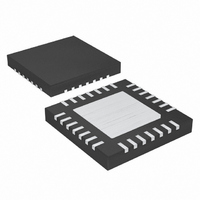
MAX8903AETI+T Maxim Integrated Products, MAX8903AETI+T Datasheet - Page 16

MAX8903AETI+T
Manufacturer Part Number
MAX8903AETI+T
Description
IC DC/DC CHARGER LI+ 28-TQFN
Manufacturer
Maxim Integrated Products
Series
Smart Power Selector™r
Datasheet
1.MAX8903AETI.pdf
(28 pages)
Specifications of MAX8903AETI+T
Function
Charge Management
Battery Type
Lithium-Ion (Li-Ion)
Voltage - Supply
4.1 V ~ 16 V
Operating Temperature
-40°C ~ 85°C
Mounting Type
Surface Mount
Package / Case
28-TQFN Exposed Pad
Lead Free Status / RoHS Status
Lead free / RoHS Compliant
2A 1-Cell Li+ DC-DC Chargers for USB
and Adapter Power
die temperature. The feedback signal requiring the
smallest current controls the average output current in
the inductor. This scheme minimizes total power dissi-
pation for battery charging and allows the battery to
absorb any load transients with minimum system volt-
age disturbance.
If the battery voltage is below V
not directly connect the system voltage to the battery
and the system voltage (V
as shown in Figure 4. The battery charger independently
controls the battery charging current. V
3.0V in the MAX8903A/MAX8903B/MAX8903E/
MAX8903G/MAX8903Y and 3.4V for MAX8903C/
MAX8903D.
After the battery charges to 50mV above V
system voltage is connected to the battery. The battery
fast-charge current then controls the step-down con-
verter to set the average inductor current so that both
the programmed input current limit and fast-charge cur-
rent limit are satisfied.
A proprietary hysteretic current PWM control scheme
ensures fast switching and physically tiny external com-
ponents. The feedback control signal that requires the
smallest input current controls the center of the peak
and valley currents in the inductor. The ripple current is
internally set to provide 4MHz operation. When the
input voltage decreases near the output voltage, very
high duty cycle occurs and, due to minimum off-time,
4MHz operation is not achievable. The controller then
provides minimum off-time, peak current regulation.
Similarly, when the input voltage is too high to allow
Table 1. External Components List for Figures 2 and 3
16
(FIGURES 2 AND 3)
COMPONENT
______________________________________________________________________________________
C
R
DC
PU
R
C
C
R
THM
C
C
, C
R
ISET
L1
BAT
SYS
IDC
VL
CT
(X4)
T
USB
DC-DC Step-Down Control Scheme
Input filter capacitor
VL filter capacitor
SYS output bypass capacitor
Battery bypass capacitor
Charger timing capacitor
Logic output pullup resistors
Negative TC thermistor
THM pullup resistor
DC input current-limit programming
Fast-charge current programming
DC input step-down inductor
SYS
) is slightly above V
SYSMIN
FUNCTION
, the charger does
SYSMIN
SYSMIN
is set to
SYSMIN
, the
4.7μF ceramic capacitor
1.0μF ceramic capacitor
10μF (MAX8903A/MAX8903C/MAX8903D/MAX8903Y) or 22μF
(MAX8903B/MAX8903E/MAX8903G) ceramic capacitor
10μF ceramic capacitor
0.15μF low TC ceramic capacitor
100kΩ
Philips NTC thermistor, P/N 2322-640-63103, 0kΩ ±5% at +25°C
10kΩ
3kΩ ±1%, for 2A limit
1.2kΩ ±1%, for 1A charging
1μH inductor with I
4MHz operation due to the minimum on-time, the con-
troller becomes a minimum on-time, valley current regu-
lator. In this way, ripple current in the inductor is always
as small as possible to reduce ripple voltage on SYS for
a given capacitance. The ripple current is made to vary
with input voltage and output voltage in a way that
reduces frequency variation. However, the frequency
still varies somewhat with operating conditions. See the
Typical Operating Characteristics .
As shown in Table 2, the DC input supports both AC
adapters (up to 2A) and USB (up to 500mA). With the
DCM logic input set high, the DC input is in adapter
mode and the DC input current limit is set by the resis-
tance from IDC to GND (R
ing to the following equation:
With the DCM logic input set low, the DC input current
limit is internally programmed to 500mA or 100mA as
set by the IUSB logic input. With the IUSB logic input
set high, the DC input current limit is 500mA and the
DC input delivers current to SYS through the step-down
regulator. With the IUSB logic input set low, the DC
input current limit is 100mA. In this 100mA mode, the
step-down regulator is turned off and its high-side
switch operates as a linear regulator with a 100mA cur-
rent limit. The linear regulator’s output is connected to
LX and its output current flows through the inductor into
CS and finally to SYS.
The DCM pin has an internal diode to DC as shown in
Figure 1. To prevent current from flowing from DCM
through the internal diode and to the DC input, DCM
SAT
> 2A
R
IDC
= 6000V/I
PART
IDC
). Calculate R
DC-MAX
DC Mode (DCM)
IDC
accord-


