DS2746G+ Maxim Integrated Products, DS2746G+ Datasheet
DS2746G+
Specifications of DS2746G+


Related parts for DS2746G+

DS2746G+ Summary of contents
Page 1
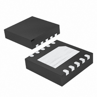
... VOUT drives Dividers, Reduces Power ±8 LSB Accuracy Active Current: 70A typical, 100A max Sleep Current: 1A typical, 3A max TEMP RANGE PIN-PACKAGE 10-Pin 3 -20ºC to +70ºC TDFN DS2746G+ in Tape- -20ºC to +70ºC and-Reel × 3mm 3mm TDFN = 15m) mm× 3mm ...
Page 2
ABSOLUTE MAXIMUM RATINGS Voltage Range on Any Pin Relative to Ground Operating Temperature Range Storage Temperature Range Soldering Temperature Stresses beyond those listed under “Absolute Maximum Ratings” may cause permanent damage to the device. These are stress ratings only, and ...
Page 3
SCL, SDA Input Capacitance: SCL, SDA Bus Low Timeout DC ELECTRICAL CHARACTERISTICS: 2-WIRE INTERFACE (V = 2.5V to 4.5V -20°C to +70°C PARAMETER SCL Clock Frequency Bus Free Time Between a STOP and START Condition Hold ...
Page 4
Figure 1. Valid Range for AIN 100% 67% 57% 48% 0% 2.5V Figure 2. 2-Wire Bus Timing Diagram Accuracy Specification GERR AINx Voltage Measurement Error ≤ AIN Specification GERR 3.7 3.86 VOUT PIN VOLTAGE ( AINx Voltage ...
Page 5
PIN DESCRIPTION PIN NAME 1 AIN1 Aux Voltage Input Number 1. 2 AIN0 Aux Voltage Input Number 0. Serial Clock Input. Input only 2-wire clock line. Connect this pin to the CLOCK signal of 3 SCL the 2-wire interface. This ...
Page 6
... Measurement registers. If sleep mode operation is enabled, holding both interface lines low forces the DS2746 into a low power sleep mode where A/D measurements are paused and the ACR register is maintained. FuelPack is a trademark of Maxim Integrated Products, Inc. after measuring the auxiliary inputs to reduce power ...
Page 7
Figure 4. APPLICATION EXAMPLE Protection IC (Li+/Polymer) 1nF 1nF POWER MODES The DS2746 operates in one of two power modes: active and sleep. While in active mode, the DS2746 operates as a high-precision battery monitor with voltage, auxiliary inputs, current ...
Page 8
Figure 5. Measurement Timing VOLTAGE MEASUREMENT Battery voltage is measured at the V voltage) and with a resolution of 2.44mV. The result is updated every 660ms with the average voltage over the last 220ms and placed in the VOLTAGE register ...
Page 9
AUXILARY INPUT MEASUREMENTS The DS2746 allows for measuring two auxiliary measurement inputs, AIN0 and AIN1, with respect to V inputs are designed for measuring resistor ratios, particularly useful for measuring thermistor or pack identification resistors time of t ...
Page 10
Table 1. Current Resolution for Various RSNS Values SNS 312.5µA 6.25V Table 2. Current Range for Various RSNS Values SNS ±51.2mV Every 1024th conversion, the ADC measures its input offset to facilitate ...
Page 11
Table 3. Accumulated Current Range for Various RSNS Values SNS 409.6mVh 20.48Ah CURRENT OFFSET BIAS The Current Offset Bias register (COBR) allows a programmable offset value to be added to raw current measurements. The result of ...
Page 12
Figure 1. Accumulation Bias Register Format MEMORY The DS2746 has memory space with registers for instrumentation, status, and control. When the MSB of a two- byte register is read, both the MSB and LSB are latched and held for the ...
Page 13
STATUS/CONFIG REGISTER The Status/Config register is read/write with individual bits designated as read only. Bit values indicate status as well as program or select device functionality. Figure 12. Status/Config Register Format BIT 7 BIT 6 X PORF X — Reserved. ...
Page 14
Bus Idle The bus is defined to be idle, or not busy, when no master device has control. Both SDA and SCL remain high when the bus is idle. The STOP condition is the proper method to return the bus ...
Page 15
Table 5. 2-Wire Protocol Key KEY DESCRIPTION S START bit SAddr Slave Address (7-bit) FCmd Function Command byte MAddr Memory Address byte Data Data byte written by master A Acknowledge bit - Master N No Acknowledge - Master Basic Transaction ...
Page 16
Data is returned beginning with the most significant bit (msb) of the data in MAddr. Because the address is automatically incremented after the least significant bit (lsb) of each byte is returned, the msb of the data at address MAddr ...
Page 17
... Maxim/Dallas Semiconductor reserves the right to change the circuitry and specifications without notice at any time The Maxim logo is a registered trademark of Maxim Integrated Products, Inc. The Dallas logo is a registered trademark of Dallas Semiconductor Corporation. DESCRIPTION maximum operating range in the DD voltage” ...