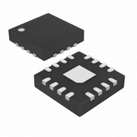
MAX4211DETE+ Maxim Integrated Products, MAX4211DETE+ Datasheet - Page 9

MAX4211DETE+
Manufacturer Part Number
MAX4211DETE+
Description
IC CURRENT MONITOR 1.5% 16TQFN
Manufacturer
Maxim Integrated Products
Datasheet
1.MAX4211BEUE.pdf
(32 pages)
Specifications of MAX4211DETE+
Function
Current Monitor
Sensing Method
High-Side
Accuracy
±1.5%
Voltage - Input
4 ~ 28 V
Operating Temperature
-40°C ~ 85°C
Mounting Type
Surface Mount
Package / Case
16-TQFN Exposed Pad
Product
Power Monitors
Supply Voltage (max)
5.5 V
Supply Voltage (min)
2.7 V
Operating Temperature Range
- 40 C to + 85 C
Mounting Style
SMD/SMT
Supply Current (max)
1100 uA
Lead Free Status / RoHS Status
Lead free / RoHS Compliant
Current - Output
-
Lead Free Status / Rohs Status
Lead free / RoHS Compliant
ELECTRICAL CHARACTERISTICS (continued)
(V
GND, V
T
*FSO refers to full-scale output under the conditions: V
Note 1:
Note 2:
Note 3:
Note 4:
Note 5:
Note 6:
Note 7:
Note 8:
Note 9:
Note 10: Total output voltage error is the sum of gain and offset voltage errors.
Note 11: POUT Output Offset Voltage is the sum of offset and multiplier feedthrough.
MAX4211B/MAX4211E (current gain = 25.00)
IOUT Gain Accuracy
Total IOUT Output Error
(Note 10)
MAX4211C/MAX4211F (current gain = 40.96)
IOUT Gain Accuracy
Total IOUT Output Error
(Note 10)
A
CC
= +25 C, unless otherwise noted.) (Note 1)
= 5.0V, V
INHIBIT
PARAMETER
All devices are 100% production tested at T
Guaranteed by power-supply rejection test.
Guaranteed by output voltage error tests (IOUT).
Guaranteed by output voltage error tests (IOUT or POUT, or both).
IN Input Voltage Range (MAX421_D/E/F) and V
(GBD) and not production tested. See Multiplier Transfer Characteristics graphs in the Typical Operating Characteristics.
This test does not apply to the low gain options, MAX421_A/D, because OUT is clamped at approximately 4V.
The device does not experience phase reversal when overdriven.
V
POUT gain accuracy is the sum of gain error and multiplier nonlinearity.
PULLUP
= 0V, R
RS+
= 25V, V
is defined as an externally applied voltage through a resistor, R
_______________________________________________________________________________________
COUT1
SENSE
= R
COUT2
∆V
∆V
∆V
∆V
= 5mV, V
SYMBOL
∆V
∆V
∆V
∆V
IOUT_MAX
IOUT
IOUT_MAX
IOUT
V
V
FSO
FSO
SENSE
IOUT
SENSE
IOUT
IOUT
IOUT
= 5k
_
_
MAX
MAX
/
/
IN
/
/
/
/
connected to V
= 1.0V, V
V
100mV, V
V
100mV
V
V
V
V
V
100mV, V
V
100mV
V
V
V
V
SENSE
SENSE
SENSE
SENSE
SENSE
SENSE
SENSE
SENSE
SENSE
SENSE
SENSE
SENSE
A
SENSE
LE
= +25°C. All temperature limits are guaranteed by design.
= 20mV to
= 5mV to
= 150mV
= 50mV
= 25mV
= 5mV
= 20mV to
= 5mV to
= 100mV
= 50mV
= 25mV
= 5mV
RS+
RS+
RS+
= 0V, R
= 100mV, V
CC
Input Voltage Range (MAX421_A/B/C) are guaranteed by design
= 25V
=25V
CONDITIONS
, T
IOUT
A
= -40 C to +85 C, unless otherwise noted. Typical values are at
= R
T
T
T
T
T
T
T
T
T
T
T
T
RS+
A
A
A
A
A
A
A
A
A
A
A
A
High-Side Power and
POUT
= +25°C
= T
= +25°C
= T
= +25°C
= T
= +25°C
= T
= +25°C
= T
= +25°C
= T
= +25V, or V
MIN
MIN
MIN
MIN
MIN
MIN
= 1M , V
to T
to T
to T
to T
to T
to T
PULLUP
Current Monitors
MAX
MAX
MAX
MAX
MAX
MAX
IN
, to pull up the comparator output.
CIN1+
= 1V.
= V
MIN
CIN2+
±0.15
±0.15
= V
TYP
±0.5
±0.2
±1.2
±1.8
±0.5
±0.2
±1.2
±1.8
±20
±20
REF
, V
MAX
±1.5
±3.0
±1.5
±3.0
±1.5
±3.0
±1.5
±3.0
±1.5
±3.0
±1.5
±3.0
CIN1-
= V
% FS O*
% FS O*
UNITS
CIN2-
%
%
%
%
=
9


