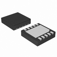
NIS5132MN2TXG ON Semiconductor, NIS5132MN2TXG Datasheet - Page 3

NIS5132MN2TXG
Manufacturer Part Number
NIS5132MN2TXG
Description
IC ELECTRONIC FUSE 12V 10DFN
Manufacturer
ON Semiconductor
Datasheet
1.NIS5132MN1TXG.pdf
(11 pages)
Specifications of NIS5132MN2TXG
Function
Electronic Fuse
Voltage - Input
9 ~ 18 V
Current - Output
3.6A
Operating Temperature
-40°C ~ 150°C
Mounting Type
Surface Mount
Package / Case
10-VFDFN Exposed Pad
Product
Power Distribution
Supply Voltage (max)
25 V
Supply Voltage (min)
- 0.6 V
Power Dissipation
1.3 W
Operating Temperature Range
- 40 C to + 150 C
Mounting Style
SMD/SMT
Lead Free Status / RoHS Status
Lead free / RoHS Compliant
Accuracy
-
Sensing Method
-
Lead Free Status / Rohs Status
Lead free / RoHS Compliant
Available stocks
Company
Part Number
Manufacturer
Quantity
Price
Company:
Part Number:
NIS5132MN2TXG
Manufacturer:
ON Semiconductor
Quantity:
500
4. Pulse test: Pulse width 300 us, duty cycle 2%.
5. Verified by design.
6. Refer to explanation of short circuit and overload conditions in application note AND8140.
7. Device will shut down prior to reaching this level based on actual UVLO trip point.
ELECTRICAL CHARACTERISTICS
unless otherwise noted.)
POWER FET
THERMAL LATCH
UNDER/OVERVOLTAGE PROTECTION
CURRENT LIMIT
dv/dt CIRCUIT
ENABLE/FAULT
TOTAL DEVICE
Delay Time (enabling of chip to I
Kelvin ON Resistance (Note 4)
T
Off State Output Voltage
(V
Output Capacitance (V
Continuous Current (T
(T
Shutdown Temperature (Note 5)
Thermal Hysteresis (Decrease in die temperature for turn on, does not
apply to latching parts)
Output Clamping Voltage (Overvoltage Protection) (V
Undervoltage Lockout (Turn on, voltage going high)
UVLO Hysteresis
Kelvin Short Circuit Current Limit (R
Kelvin Overload Current Limit (R
Output Voltage Ramp Time (Enable to V
Maximum Capacitor Voltage
Logic Level Low (Output Disabled)
Logic Level Mid (Thermal Fault, Output Disabled)
Logic Level High (Output Enabled)
High State Maximum Voltage
Logic Low Sink Current (V
Logic High Leakage Current for External Switch (V
Maximum Fanout for Fault Signal (Total number of chips that can be
connected to this pin for simultaneous shutdown)
Bias Current (Operational)
Bias Current (Shutdown)
Minimum Operating Voltage (Notes 5 and 7)
J
A
CC
= 140°C (Note 5)
= 80°C, minimum copper)
= 18 V
dc
, V
GS
= 0 V
A
DS
= 25°C, 0.5 in
dc
= 12 V
enable
Characteristics
, R
L
= R)
D
= 0 V)
dc
Limit
= 100 mA with 1 A resistive load)
, V
Limit
= 15.4 W, Note 6)
GS
2
pad) (Note 5)
OUT
= 15.4 W, Note 6)
= 0 V
(Unless otherwise noted: V
= 11.7 V)
dc
, f = 1 MHz)
enable
CC
= 18 V)
= 3.3 V)
http://onsemi.com
3
CC
= 12 V, C
Symbol
V
V
I
V
I
V
V
V
I
R
Lim−SS
Lim−OL
I
T
V
in−leak
V
in−high
in−max
in−low
V
t
I
I
T
T
Clamp
in−low
in−mid
Fan
V
UVLO
slew
DSon
Bias
Bias
Hyst
Hyst
I
I
max
min
SD
dly
off
D
D
L
= 100 mF, dv/dt pin open, R
2.75
0.35
0.82
1.96
3.40
Min
150
7.7
0.5
35
14
−
0.80
3.44
0.58
2.64
4.30
Typ
220
190
250
175
−17
1. 8
3.6
1.7
8.5
4.6
0.9
1.4
1.0
44
62
45
15
LIMIT
= 10 W, T
Max
16.2
4.25
V
0.81
1.95
3.30
300
200
−25
9.3
1.8
5.2
1.0
3.0
2.5
7.6
55
−
CC
j
= 25°C
Units
Unit
mW
mV
mA
mA
ms
mA
mA
pF
°C
°C
ms
A
V
V
V
A
A
V
V
V
V
V
V


