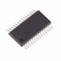
MAX6921AUI+T Maxim Integrated Products, MAX6921AUI+T Datasheet - Page 7

MAX6921AUI+T
Manufacturer Part Number
MAX6921AUI+T
Description
IC DRVR VFD TUBE SRL 28-TSSOP
Manufacturer
Maxim Integrated Products
Datasheet
1.MAX6921AUIT.pdf
(13 pages)
Specifications of MAX6921AUI+T
Display Type
Vacuum Fluorescent (VF)
Interface
4-Wire Serial
Current - Supply
1.65mA
Voltage - Supply
8 V ~ 76 V
Operating Temperature
-40°C ~ 125°C
Mounting Type
Surface Mount
Package / Case
28-TSSOP
Lead Free Status / RoHS Status
Lead free / RoHS Compliant
Configuration
-
Digits Or Characters
-
Lead Free Status / Rohs Status
Details
Figure 2. MAX6921 CMOS Output Driver Structure
The MAX6921/MAX6931 are VFD tube drivers compris-
ing a 4-wire serial interface driving 20 high-voltage rail-
to-rail output ports. The driver is suitable for both static
and multiplexed displays.
The output ports feature high current-sourcing capabili-
ty to drive current into grids and anodes of static or
multiplex VFDs. The ports also have active current sink-
ing for fast discharge of capacitive display electrodes
in multiplexing applications.
The 4-wire serial interface comprises a 20-bit shift reg-
ister and a 20-bit transparent latch. The shift register is
written through a clock input CLK and a data input DIN.
For the MAX6921, the data propagates to a data output
DOUT. The data output allows multiple drivers to be
cascaded and operated together. The output latch is
transparent to the shift register outputs when LOAD is
high, and latches the current state on the falling edge
of LOAD.
Each driver output is a slew-rated controlled CMOS
push-pull switch driving between V
(MAX6921) or V
always slower than the output fall time to avoid shoot-
through currents during output transitions. The output
slew rates are slow enough to minimize EMI, yet are
fast enough so as not to impact the typical 100µs digit
multiplex period and affect the display intensity.
An internal reset circuit clears the internal registers of
the MAX6921/MAX6931 on power-up. All outputs OUT0
to OUT19 and the interface output DOUT (MAX6921
only) initialize low regardless of the initial logic levels of
the CLK, DIN, BLANK, and LOAD inputs.
Initial Power-Up and Operation
SS
SLEW-RATE
CONTROL
_______________________________________________________________________________________
(MAX6931). The output rise time is
Detailed Description
V
BB
40Ω
TYPICAL
750Ω
TYPICAL
OUT_
20-Output, 76V, Serial-Interfaced
BB
and GND
The MAX6921/MAX6931 use 4-wire serial interface with
three inputs (DIN, CLK, LOAD) and a data output
(DOUT, MAX6921 only). This interface is used to write
output data to the MAX6921/MAX6931 (Figure 4) (Table
1). The serial interface data word length is 20 bits,
D0–D19.
The functions of the four serial interface pins are:
• CLK input is the interface clock, which shifts data
• LOAD input passes data from the MAX6921/
• DIN is the interface data input, and must be stable
• DOUT is the interface data output, which shifts data
A fifth input, BLANK, can be taken high to force outputs
OUT0 to OUT19 low, without altering the contents of the
output latches. When the BLANK input is low, outputs
OUT0 to OUT19 follow the state of the output latches. A
common use of the BLANK input is PWM intensity control.
The BLANK input’s function is independent of the oper-
ation of the serial interface. Data can be shifted into the
serial interface shift register and latched regardless of
the state of BLANK.
Figure 3. MAX6931 CMOS Output Driver Structure
into the MAX6921/MAX6931s’ 20-bit shift register on
its rising edge.
MAX6931s’ 20-bit shift register to the 20-bit output
latch when LOAD is high (transparent latch), and
latches the data on LOAD’s falling edge
when it is sampled on the rising edge of CLK.
out from the MAX6921’s 20-bit shift register on the
rising edge of CLK. Data at DIN is propagated
through the shift register and appears at DOUT (20
CLK cycles + t
VFD Tube Drivers
SLEW-RATE
DO
CONTROL
) later.
4-Wire Serial Interface
V
V
BB
SS
40Ω
TYPICAL
750Ω
TYPICAL
OUT_
7


