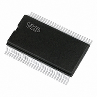
PCF8576T/1,118 NXP Semiconductors, PCF8576T/1,118 Datasheet - Page 8

PCF8576T/1,118
Manufacturer Part Number
PCF8576T/1,118
Description
IC LCD DRV UNVRSL LOW-MUX 56VSOP
Manufacturer
NXP Semiconductors
Datasheet
1.PCF8576T1118.pdf
(44 pages)
Specifications of PCF8576T/1,118
Package / Case
56-VSOP
Display Type
LCD
Configuration
40 Segment
Interface
I²C
Current - Supply
180µA
Voltage - Supply
2 V ~ 9 V
Operating Temperature
-40°C ~ 85°C
Mounting Type
Surface Mount
Number Of Digits
20
Number Of Segments
160
Maximum Clock Frequency
288 KHz
Operating Supply Voltage
2 V to 9 V
Maximum Power Dissipation
400 mW
Maximum Supply Current
180 uA
Lead Free Status / RoHS Status
Lead free / RoHS Compliant
Digits Or Characters
-
Lead Free Status / Rohs Status
Lead free / RoHS Compliant
Other names
933804620118
PCF8576T/1-T
PCF8576T/1-T
PCF8576T/1-T
PCF8576T/1-T
Philips Semiconductors
6.1
At power-on the PCF8576 resets to a starting condition as
follows:
1. All backplane outputs are set to V
2. All segment outputs are set to V
3. The drive mode ‘1 : 4 multiplex with
4. Blinking is switched off.
5. Input and output bank selectors are reset (as defined
6. The I
7. The data pointer and the subaddress counter are
Data transfers on the I
following power-on to allow completion of the reset action.
6.2
The full-scale LCD voltage (V
V
compensated externally through the V
Fractional LCD biasing voltages are obtained from an
internal voltage divider of the three series resistors
connected between V
be switched out of the circuit to provide a
level for the 1 : 2 multiplex configuration.
Table 1 Preferred LCD drive modes: summary of characteristics
2001 Oct 02
static
1 : 2
1 : 2
1 : 3
1 : 4
DD
LCD DRIVE MODE
Universal LCD driver for low multiplex rates
in Table 4).
cleared.
V
Power-on reset
LCD bias generator
LCD
2
C-bus interface is initialized.
. The LCD voltage may be temperature
DD
2
C-bus should be avoided for 1 ms
BACKPLANES
and V
1
2
2
3
4
op
LCD
) is obtained from
. The centre resistor can
NUMBER OF
DD
LCD
DD
.
1
.
3
supply to pin 12.
bias’ is selected.
1
2
bias voltage
LEVELS
2
3
4
4
4
8
CONFIGURATION
6.3
The LCD voltage selector co-ordinates the multiplexing of
the LCD in accordance with the selected LCD drive
configuration. The operation of the voltage selector is
controlled by MODE SET commands from the command
decoder. The biasing configurations that apply to the
preferred modes of operation, together with the biasing
characteristics as functions of V
resulting discrimination ratios (D), are given in Table 1.
A practical value for V
with a defined LCD threshold voltage (V
the LCD exhibits approximately 10% contrast. In the static
drive mode a suitable choice is V
Multiplex drive ratios of 1 : 3 and 1 : 4 with
possible but the discrimination and hence the contrast
ratios are smaller (
The advantage of these modes is a reduction of the LCD
full-scale voltage V
These compare with V
----------
3
21
1 : 3 multiplex (
V
1 : 4 multiplex (
V
LCD BIAS
op
op
static
= 1.528 for 1 : 4 multiplex).
=
=
1
1
1
1
LCD voltage selector
2
3
3
3
--------------------- -
6 V
4
3
off rms
3
1
1
op
2
2
bias):
bias):
3
= 2.309 V
V
-------------------- -
op
as follows:
0
0.354
0.333
0.333
0.333
off(rms)
op
V
= 1.732 for 1 : 3 multiplex or
= 2.449 V
is determined by equating V
op
= 3 V
off(rms)
off(rms)
op
V
-------------------- -
op
off(rms)
1
0.791
0.745
0.638
0.577
on(rms)
V
= V
> 3V
op
Product specification
when
DD
th
th
PCF8576
), typically when
approximately.
V
1
1
D
3
LCD
2
bias are
bias is used.
=
2.236
2.236
1.915
1.732
and the
V
-------------------- -
V
on(rms)
off(rms)
off(rms)


