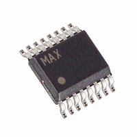
MAX6852AEE+T Maxim Integrated Products, MAX6852AEE+T Datasheet - Page 18

MAX6852AEE+T
Manufacturer Part Number
MAX6852AEE+T
Description
IC VFD CTRLR MATRIX 16QSOP
Manufacturer
Maxim Integrated Products
Datasheet
1.MAX6852AEET.pdf
(32 pages)
Specifications of MAX6852AEE+T
Display Type
Vacuum Fluorescent (VF)
Configuration
5 x 7 (Matrix)
Interface
Serial
Current - Supply
3.5mA
Voltage - Supply
2.7 V ~ 3.6 V
Operating Temperature
-40°C ~ 125°C
Mounting Type
Surface Mount
Package / Case
16-QSOP
Lead Free Status / RoHS Status
Lead free / RoHS Compliant
Digits Or Characters
-
4-Wire Interfaced, 5
Fluorescent Display Controller
The output map is an indirect addressing reference
table. It translates bit position in the output shift register
(valid range: from zero to the value in shift-limit register
0x0E) to bit function. Any output shift-register bit posi-
tion may be set to any grid, 5 x 7 matrix segment, DP
segment, annunciator segment, or cursor segment.
The power-up default pattern for output map RAM
maps a 40-digit, two-digits-per-grid display with DPs
and cursors (Table 30).
If the user selects an unused map RAM entry (126 or
127) for an output shift-register position, then the corre-
sponding output bit is always low (segment or grid OFF).
When selecting an invalid map RAM entry (for example,
codes 48 to 83 to select annunciators in 96/2 mode,
which does not support annunciators), the correspond-
ing output bit is always low (segment or grid OFF).
If the map RAM entry corresponds to a nonexistent font
segment (no action in Table 30) when the digit data is
processed through the character font, then the result
again is zero (segment or grid OFF).
The output map data is indirectly accessed by an
autoincrementing output map address pointer in the
MAX6852 at address 0x06. The output map address
pointer can be written (i.e., set to an address between
0x00 and 0x79) but cannot be read back. The output
map data is written and read back through the output
map address pointer.
Table 31 shows how to set the output map address
pointer to a value within the acceptable range. Bit D7 is
set to denote that the user is writing the output map
address pointer. If the user attempts to set the output
map address to one of the out-of-range addresses by
writing data in range 0xFA to 0xFF, then address 0x00
is set instead.
After the last data location 0xF9 has been written, fur-
ther output map data entries are ignored until the out-
put map address pointer is reset.
The output map data can be written to the address set
by the output map address pointer. Bit D7 is clear to
denote that the user is writing actual output map data.
The output map address pointer is autoincremented
after the output map data has been written to the cur-
rent location. If the user writes the output map data in
the RAM order, then the output map address pointer
need only be set once, or even not at all as the address
is set to 0x00 as power-up default (Table 32).
The output map data can be read by reading address
0x86. The 7-bit output map data at the address set by
the output map address pointer is read back, with the
MSB clear. The output map address pointer is autoin-
18
______________________________________________________________________________________
✕
7 Matrix Vacuum-
cremented after the output map data has been read
from the current location, in the same way as for a write
(Table 33).
The VFD filament is typically driven with an AC wave-
form, supplied by a center-tapped 50Hz or 60Hz power
transformer as part of the system power supply.
However, if the system has only DC supplies available,
the filament must be powered by a DC-AC or DC-DC
converter.
The MAX6852 can generate the waveforms on the
PHASE1 and PHASE2 outputs to drive the VFD filament
using a full bridge (push-pull drive). The PHASE1 and
PHASE2 outputs can be used as general-purpose out-
puts if the filament drive is not required. The bridge
drive transistors are external, but the waveforms are
generated by the MAX6852.
The waveform generation uses PWM to set the effective
RMS voltage across the filament, as a fraction of the
external supply voltage (Figure 13) (Table 34). The fila-
ment switching frequency is synchronized to the multi-
plex scan clock, eliminating beating artifacts due to
differing filament and multiplex frequencies.
The PWM duty cycle is controlled by the filament duty-
cycle register (Table 35). The effective RMS voltage
across the filament is given by the expression:
V
or, rearranged:
Duty = 200 x V
where:
FilOn is the number to store in the filament duty-cycle
register, address 0x09.
V
V
V
bridge driver (V).
V
bridge driver (V).
The minimum commutation time, shown at (C) in Figure
13, is set by (2/OSC)s (500ns when OSC = 4MHz) to
ensure that shoot-through currents cannot flow during
phase reversal. Otherwise, the duty cycle of the bridge
(total on time: total time) sets the RMS voltage across
the filament. This technique provides a low-cost AC fila-
ment supply when using a regulated supply higher than
the RMS voltage rating of the filament.
RMS
FIL
RMS
LO-BRIDGE
HI-BRIDGE
is the supply voltage to the filament driver bridge (V).
is the specified nominal filament supply voltage (V).
= FilOn x (V
is the voltage drop across a high-side
is the voltage drop across a low-side
RMS
FIL
/ (V
- V
FIL
LO-BRIDGE
- V
LO-BRIDGE
- V
Filament Drive
HI-BRIDGE
- V
HI-BRIDGE
) / 200
)


