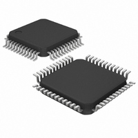
MAX1368ECM+T Maxim Integrated Products, MAX1368ECM+T Datasheet - Page 31

MAX1368ECM+T
Manufacturer Part Number
MAX1368ECM+T
Description
IC PANEL METER 3.5 DIG 48LQFP
Manufacturer
Maxim Integrated Products
Datasheet
1.MAX1368ECM.pdf
(36 pages)
Specifications of MAX1368ECM+T
Display Type
LED
Configuration
7 Segment
Interface
Serial
Digits Or Characters
A/D 3.5 Digits
Voltage - Supply
2.7 V ~ 5.25 V
Operating Temperature
-40°C ~ 85°C
Mounting Type
Surface Mount
Package / Case
48-LQFP
Lead Free Status / RoHS Status
Lead free / RoHS Compliant
Current - Supply
-
The transfer function for the MAX1366 with AIN+ - AIN-
< 0 and RANGE = DV
The transfer function for the MAX1368 with AIN+ - AIN-
≥ 0 and RANGE = DV
The transfer function for the MAX1368 with AIN+ - AIN-
< 0 and RANGE = DV
Figure 20
MAX1366/MAX1368 in unipolar and bipolar modes.
The transfer function for the DAC in the MAX1366/
MAX1368 unipolar mode is:
where N = two’s complement ADC output code.
In unipolar mode, V
complement ADC codes less than zero (see
The transfer function for the DAC in the MAX1366/
MAX1368 in bipolar mode is:
where N = two’s complement ADC output.
A user can independently write to the DAC but cannot
input codes greater than +19,999 or less than -19,999.
In bipolar mode, a -19,999 DAC code provides 4mA
(0mA) output current and a +19,999 DAC code pro-
vides a 20mA (16mA) output current.
Figures 20 and 21
fer function of the output current (4-20OUT) versus the
ADC output code.
Note: The input at V
dence of typically 6kΩ when driving V
( )
( )
6
( )
7
8
COUNT
COUNT
COUNT
Microcontroller-Interface, 4.5-/3.5-Digit Panel
shows the DAC transfer function for the
V
=
=
=
DACVOUT
V
1 024
DACVOUT
1 024
1 024
Voltage-to-Current Transfer Function
.
.
.
Writing into the DAC Independently
______________________________________________________________________________________
show the MAX1366/MAX1368 trans-
DACVOUT
DD
CONV_IN
DD
DD
V
V
V
V
V
V
REF
=
AIN
REF
REF
AIN
is:
AIN
is:
is:
=
N
+ −
+ −
32 768 1
+19 999
+ −
+ −
+ −
+ −
6536
is equal to 0V for all two’s
DAC Transfer Functions
,
expects a source impe-
,
V
V
N
V
V
V
V
AIN
REF
AIN
REF
AIN
REF
−
−
−
−
CONV_IN
−
−
x V
−
x V
x
x
x
REF
20 000
2000
2000
REF
,
Figure
externally.
x
x
x
10
10 1
Meters with 4–20mA Output
10 1
+
21).
+
Figure 23
tion of the output current (4-20OUT) versus the input
voltage of the V/I converter.
The transfer function for the MAX1366/MAX1368 with
the current offset enabled (EN_I is high) is:
The transfer function for the MAX1366/MAX1368 with
the current offset disabled (EN_I is low) is:
Power up AV
input and external-reference voltage to the device. If
this is not possible, limit the current into these inputs to
50mA. When the analog and digital supplies come from
the same source, isolate the digital supply from the
analog supply with a low-value resistor (10Ω) or ferrite
bead. For best performance, ground the MAX1366/
MAX1368 to the analog ground plane of the circuit
board. Avoid running digital lines under the device as
this can couple noise onto the IC. Run the analog
ground plane under the MAX1366/MAX1368 to mini-
mize coupling of digital noise. Make the power-supply
lines to the MAX1366/MAX1368 as wide as possible to
provide low-impedance paths and reduce the effects of
glitches on the power-supply line. Shield fast-switching
signals, such as clocks, with digital ground to avoid
radiating noise to other sections of the board. Avoid
running clock signals near the analog inputs. Avoid
crossover of digital and analog signals. Running traces
that are on opposite sides of the board at right angles to
each other reduces feedthrough effects. A microstrip
technique is best, but is not always possible with dou-
ble-sided boards. With this technique, the component
side of the board is dedicated to ground planes while
signals are placed on the solder side. Good decoupling
is important when using high-resolution ADCs.
Decouple the supplies with 0.1µF ceramic capacitors to
GND. Place these components as close to the device
as possible to achieve the best decoupling.
A resistor from ISET to ground sets the current for each
LED segment. See
lowing formula to set the segment current:
IOUT
≅
16
1 25
.
mA
shows the MAX1366/MAX1368 transfer func-
DD
Supplies, Layout, and Bypassing
x V
I
SEG
and DV
IOUT
CONV IN
Table 7
Selecting Segment Current
=
≅
_
1 20
R
DD
16
.
1 25
ISET
.
mA
+
for more detail. Use the fol-
before applying an analog
V
4
mA
x
x V
400
CONV IN
_
31


