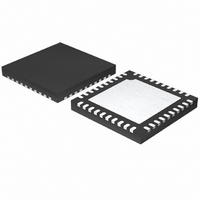
MAX6955ATL+T Maxim Integrated Products, MAX6955ATL+T Datasheet - Page 15

MAX6955ATL+T
Manufacturer Part Number
MAX6955ATL+T
Description
IC DRVR DSPL LED 40-TQFN
Manufacturer
Maxim Integrated Products
Datasheet
1.MAX6955AAX.pdf
(43 pages)
Specifications of MAX6955ATL+T
Display Type
LED
Configuration
7, 14, 16 Segment
Interface
I²C
Current - Supply
22mA
Voltage - Supply
2.7 V ~ 5.5 V
Operating Temperature
-40°C ~ 125°C
Mounting Type
Surface Mount
Package / Case
40-TQFN Exposed Pad
Number Of Digits
16
Number Of Segments
128
Low Level Output Current
935 mA
High Level Output Current
55 mA
Operating Supply Voltage
2.7 V to 5.5 V
Maximum Supply Current
30 mA
Maximum Power Dissipation
2051.3 mW
Maximum Operating Temperature
+ 125 C
Mounting Style
SMD/SMT
Minimum Operating Temperature
- 40 C
Lead Free Status / RoHS Status
Lead free / RoHS Compliant
Digits Or Characters
-
Lead Free Status / Rohs Status
Details
One diode is required per key switch. Note that the for-
ward voltages of the diode and LED must exceed V
of P0–P3. If this condition is not met, the voltage input
to the port might be lower than the logic threshold and
keys will not be detected properly.
The MAX6955 can only scan the maximum 32 keys if
the scan-limit register is set to scan the maximum eight
digits. If the MAX6955 is driving fewer digits, then a
maximum of (4 x n) switches can be scanned, where n
is the number of digits set in the scan-limit register. For
example, if the MAX6955 is driving four 14-segment
digits, cathode drivers O0 to O3 are used. Only 16 keys
can be scanned in this configuration; the switches
shown connected to O4 through O7 are not read.
If the user wishes to scan fewer than 32 keys, then
fewer scan lines can be configured for key scanning.
The unused Key_x ports are released back to their orig-
inal GPIO functionality. If key scanning is enabled,
Table 7. Register Address Map (continued)
Note: Unused register bits read as zero.
Figure 5. Bit Transfer
SDA
SCL
Write Digit 2a Planes P0 and P1 with Same
Data (7 Segment Only), Reads as 0x00
Write Digit 3a Planes P0 and P1 with Same
Data (7 Segment Only), Reads as 0x00
Write Digit 4a Planes P0 and P1 with Same
Data (7 Segment Only), Reads as 0x00
Write Digit 5a Planes P0 and P1 with Same
Data (7 Segment Only), Reads as 0x00
Write Digit 6a Planes P0 and P1 with Same
Data (7 Segment Only), Reads as 0x00
Write Digit 7a Planes P0 and P1 with Same
Data (7 Segment Only), Reads as 0x00
DATA LINE STABLE,
DATA VALID
2-Wire Interfaced, 2.7V to 5.5V LED Display
REGISTER
______________________________________________________________________________________
Driver with I/O Expander and Key Scan
CHANGE OF DATA
ALLOWED
D15
X
X
X
X
X
X
D14
1
1
1
1
1
1
IH
ADDRESS (COMMAND BYTE)
D13
1
1
1
1
1
1
regardless of the number of keys being scanned,
P4/IRQ is always configured as IRQ (Table 32).
The key-scanning circuit utilizes the LEDs’ common-
cathode driver outputs as the key-scan drivers. O0 to
O7 go low for nominally 200µs (with OSC = 4MHz) in
turn as the displays are multiplexed. By varying the
oscillator frequency, the debounce time changes,
though key scanning still functions. Key_x inputs have
internal pullup resistors that allow the key condition to
be tested. The Key_x input is low during the appropri-
ate digit multiplex period when the key is pressed. The
timing diagram of Figure 12 shows the normal situation
where all eight LED cathode drivers are used.
Figure 6. Acknowledge
BY TRANSMITTER
BY RECEIVER
D12
0
0
0
0
0
0
START CONDITION
SCL
SDA
SDA
D11
1
1
1
1
1
1
S
D10
0
0
1
1
1
1
CLOCK PULSE FOR ACKNOWLEDGMENT
1
D9
1
1
0
0
1
1
2
D8
0
1
0
1
0
1
8
HEX CODE
0x6C
0x6D
0x6A
0x6B
0x6E
0x6F
9
15


