MM5451N National Semiconductor, MM5451N Datasheet - Page 4
MM5451N
Manufacturer Part Number
MM5451N
Description
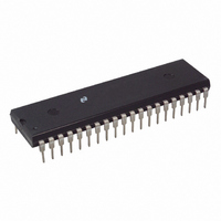
IC LED DISPLAY DRIVER 40DIP
Manufacturer
National Semiconductor
Datasheet
1.MM5450N.pdf
(8 pages)
Specifications of MM5451N
Display Type
LED
Configuration
7 Segment
Interface
Serial
Digits Or Characters
4 or 5 Digits
Current - Supply
7mA
Voltage - Supply
4.75 V ~ 11 V
Operating Temperature
-25°C ~ 85°C
Mounting Type
Through Hole
Package / Case
40-DIP (0.600", 15.24mm)
Lead Free Status / RoHS Status
Contains lead / RoHS non-compliant
Other names
*MM5451N
Available stocks
Company
Part Number
Manufacturer
Quantity
Price
Company:

Part Number:
MM5451N
Manufacturer:
LINEAR
Quantity:
10 566


Figure 4 shows the input data format A start bit of logical
Functional Description
Both the MM5450 and the MM5451 are specifically de-
signed to operate 4- or 5-digit alphanumeric displays with
minimal interface with the display and the data source Seri-
al data transfer from the data source to the display driver is
accomplished with 2 signals serial data and clock Using a
format of a leading ‘‘1’’ followed by the 35 data bits allows
data transfer without an additional load signal The 35 data
bits are latched after the 36th bit is complete thus providing
non-multiplexed direct drive to the display Outputs change
only if the serial data bits differ from the previous time Dis-
play brightness is determined by control of the output cur-
rent for LED displays A 0 001 capacitor should be connect-
ed to brightness control pin 19 to prevent possible oscilla-
tions
A block diagram is shown in Figure 1 For the MM5450 a
DATA ENABLE is used instead of the 35th output The
DATA ENABLE input is a metal option for the MM5450 The
output current is typically 20 times greater than the current
into pin 19 which is set by an external variable resistor
There is an internal limiting resistor of 400X nominal value
‘‘1’’ precedes the 35 bits of data At the 36th clock a LOAD
signal is generated synchronously with the high state of the
clock which loads the 35 bits of the shift registers into the
latches At the low state of the clock a RESET signal is
generated which clears all the shift registers for the next set
of data The shift registers are static master-slave configura-
tion There is no clear for the master portion of the first shift
register thus allowing continuous operation
FIGURE 3
4
Figure 2 shows the pin-out of the MM5450 and MM5451 Bit
Figure 3 shows the timing relationships between data clock
Figure 7
There must be a complete set of 36 clocks or the shift regis-
ters will not clear
When the chip first powers ON an internal power ON reset
signal is generated which resets all registers and all latches
The START bit and the first clock return the chip to its nor-
mal operation
1 is the first bit following the start bit and it will appear on pin
18 A logical ‘‘1’’ at the input will turn on the appropriate
LED
and DATA ENABLE A max clock frequency of 0 5 MHz is
assumed
For applications where a lesser number of outputs are used
it is possible to either increase the current per output or
operate the part at higher than 1V V
equation can be used for calculations
T
where
The above equation was used to plot Figure 5 Figure 6 and
j
T
V
I
i
T
i
i
e
LED
JA
JA
JA
j
OUT
A
e
(V
e
(Socket Mount)
(Board Mount)
e
e
junction temperature 150 C max
OUT
ambient temperature
e
thermal coefficient of the package
the LED current
the voltage at the LED driver outputs
) (I
LED
) (No of segments)(i
e
e
49 C W
54 C W
OUT
JA
TL F 6136–4
)
a
The following
T
A
Related parts for MM5451N
Image
Part Number
Description
Manufacturer
Datasheet
Request
R

Part Number:
Description:
National Semiconductor [8-Bit D/A Converter]
Manufacturer:
National Semiconductor
Datasheet:
Part Number:
Description:
National Semiconductor [Media Coprocessor]
Manufacturer:
National Semiconductor
Datasheet:
Part Number:
Description:
Digitally Controlled Tone and Volume Circuit with Stereo Audio Power Amplifier, Microphone Preamp Stage and National 3D Sound
Manufacturer:
National Semiconductor
Datasheet:
Part Number:
Description:
Digitally Controlled Tone and Volume Circuit with Stereo Audio Power Amplifier, Microphone Preamp Stage and National 3D Sound
Manufacturer:
National Semiconductor
Datasheet:
Part Number:
Description:
AC97 Rev 2 Codec with Sample Rate Conversion and National 3D Sound
Manufacturer:
National Semiconductor
Part Number:
Description:
Manufacturer:
National Semiconductor
Datasheet:
Part Number:
Description:
Manufacturer:
National Semiconductor
Datasheet:
Part Number:
Description:
General Purpose, Low Voltage, Low Power, Rail-to-Rail Output Operational Amplifiers
Manufacturer:
National Semiconductor
Datasheet:
Part Number:
Description:
8-bit 20 MSPS flash A/D converter.
Manufacturer:
National Semiconductor
Datasheet:
Part Number:
Description:
Low Noise Quad Operational Amplifier
Manufacturer:
National Semiconductor
Datasheet:
Part Number:
Description:
Quad Differential Line Receivers
Manufacturer:
National Semiconductor
Datasheet:
Part Number:
Description:
Quad High Speed Trapezoidal? Bus Transceiver
Manufacturer:
National Semiconductor
Datasheet:
Part Number:
Description:
Dual Line Receiver
Manufacturer:
National Semiconductor
Datasheet:
Part Number:
Description:
TTL to 10k ECL Level Translator with Latch
Manufacturer:
National Semiconductor
Datasheet: