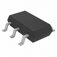
LTC4210-2IS6#TRMPBF Linear Technology, LTC4210-2IS6#TRMPBF Datasheet - Page 6

LTC4210-2IS6#TRMPBF
Manufacturer Part Number
LTC4210-2IS6#TRMPBF
Description
IC CONTROLLER HOT SWAP TSOT23-6
Manufacturer
Linear Technology
Type
Hot-Swap Controllerr
Datasheet
1.LTC4210-1CS6TRMPBF.pdf
(20 pages)
Specifications of LTC4210-2IS6#TRMPBF
Applications
General Purpose
Internal Switch(s)
No
Voltage - Supply
2.7 V ~ 16.5 V
Operating Temperature
-40°C ~ 85°C
Mounting Type
Surface Mount
Package / Case
SOT-23-6 Thin, TSOT-23-6
Linear Misc Type
Positive Low Voltage
Family Name
LTC4210-2
Package Type
TSOT-23
Operating Supply Voltage (min)
2.7V
Operating Supply Voltage (max)
16.5V
Operating Temperature (min)
-40C
Operating Temperature (max)
85C
Operating Temperature Classification
Industrial
Product Height (mm)
0.9mm
Product Length (mm)
2.9mm
Mounting
Surface Mount
Pin Count
6
Lead Free Status / RoHS Status
Lead free / RoHS Compliant
Other names
LTC4210-2IS6#TRMPBFTR
Available stocks
Company
Part Number
Manufacturer
Quantity
Price
PI FU CTIO S
LTC4210-1/LTC4210-2
TIMER (Pin 1): Timer Input Pin. An external capacitor
C
the TIMER pin is pulled beyond the COMP2 threshold,
such as for overvoltage detection with an external zener.
GND (Pin 2): Ground Pin.
ON (Pin 3): ON Input Pin. The ON pin comparator has a
low-to-high threshold of 1.3V with 80mV hysteresis and a
glitch filter. When the ON pin is low, the LTC4210 is reset.
When the ON pin goes high, the GATE turns on after the
initial timing cycle.
GATE (Pin 4): GATE Output Pin. This pin is the high side
gate drive of an external N-channel MOSFET. An internal
charge pump provides a 10 A pull-up current with Zener
clamps to V
TYPICAL PERFOR A CE CHARACTERISTICS
6
F circuit breaker delay. The GATE pin turns off whenever
TIMER
U
sets a 272.9ms/ F initial timing delay and a 21.7ms/
U
CC
and ground. In overload, the error amplifier
58
56
54
52
50
48
46
44
42
0
V
U
T
CB
A
= 25 C
2
vs Supply Voltage
4
W
SUPPLY VOLTAGE (V)
6
8
U
10
12
14
16
18
4210 G24
20
(EA) controls the external MOSFET to maintain a constant
load current. An external R-C compensation network
should be connected to this pin for current limit loop
stability.
SENSE (Pin 5): Current Limit Sense Input Pin. A sense
resistor between the V
current limit. In overload, the EA controls the external
MOSFET gate to maintain the SENSE pin voltage at 50mV
below V
TIMER circuit breaker mode is activated. The current limit
loop/circuit breaker mode can be disabled by connecting
the SENSE pin to the V
V
supply voltage range is between 2.7V to 16.5V. An under-
voltage lockout (UVLO) circuit with a glitch filter resets the
LTC4210 when a low supply voltage is detected.
CC
(Pin 6): Positive Supply Input Pin. The operating
58
56
54
52
50
48
46
44
42
CC
–75
V
. When the EA is maintaining current limit, the
CB
V
CC
–50
vs Temperature
= 5V
–25
TEMPERATURE ( C)
0
CC
25
CC
and SENSE pins sets the analog
pin.
50
75 100 125
4210 G25
150
421012f


