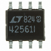
LT4256-1IS8#PBF Linear Technology, LT4256-1IS8#PBF Datasheet - Page 8

LT4256-1IS8#PBF
Manufacturer Part Number
LT4256-1IS8#PBF
Description
IC CTLR HOTSWAP HV LATCH 8SOIC
Manufacturer
Linear Technology
Type
Hot-Swap Controllerr
Datasheet
1.LT4256-2CS8PBF.pdf
(16 pages)
Specifications of LT4256-1IS8#PBF
Applications
General Purpose
Internal Switch(s)
No
Voltage - Supply
10.8 V ~ 80 V
Operating Temperature
-40°C ~ 85°C
Mounting Type
Surface Mount
Package / Case
8-SOIC (0.154", 3.90mm Width)
Lead Free Status / RoHS Status
Lead free / RoHS Compliant
Available stocks
Company
Part Number
Manufacturer
Quantity
Price
APPLICATIO S I FOR ATIO
LT4256-1/LT4256-2
TEST CIRCUIT
Hot Circuit Insertion
When circuit boards are inserted into a live backplane, the
supply bypass capacitors on the boards draw high peak
currents from the backplane power bus as they charge.
The transient currents can permanently damage the con-
nector pins and glitch the system supply, causing other
boards in the system to reset.
The LT4256-1/LT4256-2 are designed to turn on a board’s
supply voltage in a controlled manner, allowing the board
to be safely inserted or removed from a live backplane. The
TI I G DIAGRA S
8
W U
GATE
UV
4V
Figure 2. UV to GATE Timing
V
U
OUT
t
PLHUV
+2V
U
W
V
CC
W
– SENSE
GATE
3.6V
Figure 4. SENSE to GATE Timing
4256 F02
V
48k
OUT
U
t
PHLUV
55mV
+2V
V
CC
PWRGD
FB
UV
t
PHLSENSE
Figure 1
GND
SENSE
TIMER
GATE
device also provides undervoltage as well as overcurrent
protection while a power good output signal indicates
when the output supply voltage is ready with a high output.
Power-Up Sequence
An external N-channel MOSFET pass transistor (Q1) is
placed in the power path to control the power up of the
supply voltage (Figure 5). Resistor R5 provides current
detection and capacitor C1 controls the GATE slew rate.
Resistor R7 compensates the current control loop while
R6 prevents high frequency oscillations in Q1.
V
CC
PWRGD
4256 F01
48V
FB
+ –
Figure 3. V
4.45V
100pF
1V
4256 F04
t
PLHFB
OUT
to PWRGD Timing
3.99V
4256 F03
1V
t
PHLFB
425612fa


