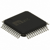
MIC2593-2YTQ Micrel Inc, MIC2593-2YTQ Datasheet - Page 12

MIC2593-2YTQ
Manufacturer Part Number
MIC2593-2YTQ
Description
IC CTRLR HOTPLUG PCI DUAL 48TQFP
Manufacturer
Micrel Inc
Type
Hot-Swap Controllerr
Datasheet
1.MIC2593-2YTQ.pdf
(26 pages)
Specifications of MIC2593-2YTQ
Applications
PCI, PCI-X
Internal Switch(s)
No
Voltage - Supply
3.3V, 5V, ±12V
Operating Temperature
0°C ~ 70°C
Mounting Type
Surface Mount
Package / Case
48-TQFP
Lead Free Status / RoHS Status
Lead free / RoHS Compliant
Other names
576-1100
Available stocks
Company
Part Number
Manufacturer
Quantity
Price
Power-Up Cycle
When a slot is off, the 5VGATE and 3VGATE pins are
held low with an internal pull-down current source. When
a slot’s MAIN outputs are enabled by applying a rising-
edge signal at the ON[A/B] control input and all input
voltages are above their respective undervoltage lockout
thresholds, all four main supplies will then execute a
controlled turn on. The 5VGATE and 3VGATE pins are
each connected to a constant current source of 25µA,
nominal. Both the 5V and 3.3V outputs act as source
followers, where:
until the associated output is equal to its input. The
voltages on the gates of the external MOSFETs for the 5V
and 3.3V MAIN supplies will continue to rise to
approximately 11.5V, ensuring minimum R
MOSFET. Note that a delay exists between the ON
command to a slot and the appearance of voltage at the
slot’s 3.3V or 5V MAIN output. This delay is the time
required to charge the 3V or 5V GATE output up to the
threshold voltage of the external MOSFET (typically about
4V). For the 5V and 3.3V MAIN supplies, the source
(output) side of the external MOSFET will reach the drain
(input) voltage in a time given by:
Table 1 provides a reference list of the expected GATE
output slew rate for the 3.3V and 5V supplies using
several (decade-scale) standard capacitors.
For the +12V and –12V supplies, the output slew rate is
controlled by capacitors connected to the 12VSLEWA and
12VSLEWB pins. To determine the minimum value of the
slew rate capacitor, (C
does not enter into current limit during start-up, the
following equation is used:
where C
+12V and –12V outputs, I
slow-trip thresholds and I
current found in the “Electrical Characteristics” table. The
slew rate dv/dt is computed by:
Micrel, Inc.
September 2008
Table 1. 3.3V/5V Output Slew Rate Selection
V
t
C
LOAD
DELAY
0.001µF
SOURCE
SLEW
0.01µF
C
0.1µF
1µF
GATE
is the load capacitance connected to the
(min)
=
=
(
C
I
[
GATE
GATE(SOURC
V
=
GATE
I
SLEW
I
LIM[12V/12
SLEW
×
I
LIM[12V/12MV]
SLEW
SLEW
−
V
= 25µA
), and to ensure the device
DRAIN
V
TH(ON)
E)
MV]
is the slew rate charge
)
×
]
are the current limit
C
dv/dt (load)
25000V/s
LOAD
2500V/s
250V/s
25V/s
DS(ON)
of the
12
By appropriately selecting the value of C
magnitude of the inrush current will not exceed the current
limit for a given load capacitance. Since one capacitor
fixes the slew rate for both +12V and –12V, the capacitor
value should be chosen to provide the slower slew rate of
the two. Table 2 depicts the ±12V output slew rate for
various values of C
Power Down Cycle
When a slot is turned off, internal switches are connected
to each of the outputs to discharge the PCI board's
bypass capacitors to ground.
Standby Mode
Standby mode is entered when any (one or more)
enabled MAIN supply input (12V
3V
MIC2593 supplies two 3.3V auxiliary outputs, VAUX[A/B],
satisfying PCI 2.x specifications. These outputs are fed
via the VSTBY[A/B] input and controlled by the
AUXEN[A/B] inputs or via their SMI bus Control Registers.
These outputs are independent of the MAIN outputs:
should one or more of the MAIN supply inputs move
below its UVLO thresholds, VAUX[A/B] will still function as
long as VSTBY[A/B] is present. Prior to entering standby
mode, ONA and ONB (or the MAINA and MAINB bits in
the Control Registers) inputs should be de-asserted. If this
is not done, the MIC2593 will assert /FAULT and also
/INT if interrupts are enabled, when the MIC2593 detects
an undervoltage condition on a supply input.
Circuit Breaker Functions
The MIC2593 provides an electronic circuit breaker
function that protects against excessive loads, such as
short circuits, at each supply. When the current from one
or more of a slot’s MAIN outputs exceeds the current limit
threshold (50mV/R
and/or 0.2A for –12V) for a duration greater than the
overcurrent timer, t
MAIN supplies (all outputs except VAUX[A/B]) are shut
off. Should the load current exceed I
12V), or cause a MAIN output’s V
(+3.3V and +5V), the outputs are shut off with no delay.
Undervoltage conditions on the MAIN supply inputs also
IN
) drops below its respective UVLO threshold. The
dv/dt
Table 2. ±12V Output Slew Rate Selection
0.001µF
0.01µF
C
0.1µF
1µF
GATE
(at
load)
FLT
SLEW
SENSE
, the circuit breaker is tripped and all
=
I
.
SLEW
for 3.3V and 5V, 1.0A for +12V,
C
SLEW
= 22µA
I
SLEW
×
IN
10
SENSE
, 12MV
6
THFAST
dv/dt (load)
0.022V/ms
0.22V/ms
to exceed V
2.2V/ms
22V/ms
M9999-092208
IN
, 5V
(+12V and –
MIC2593
SLEW
IN
and/or
, the
THFAST


