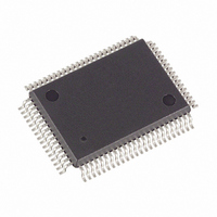
MAX5959AECS+ Maxim Integrated Products, MAX5959AECS+ Datasheet - Page 21

MAX5959AECS+
Manufacturer Part Number
MAX5959AECS+
Description
IC CTRLR HOT-PLUG QD 80-TQFP
Manufacturer
Maxim Integrated Products
Type
Hot-Swap Controllerr
Datasheet
1.MAX5959AECS.pdf
(25 pages)
Specifications of MAX5959AECS+
Applications
General Purpose, PCI Express
Internal Switch(s)
No
Voltage - Supply
3.3V, 12V
Operating Temperature
-40°C ~ 85°C
Mounting Type
Surface Mount
Package / Case
80-TQFP, 80-VQFP
Product
Controllers & Switches
Supply Voltage (max)
13 V
Supply Voltage (min)
3.3 V
Power Dissipation
1860 mW
Operating Temperature Range
- 40 C to + 85 C
Mounting Style
SMD/SMT
Supply Current
1 mA
Lead Free Status / RoHS Status
Lead free / RoHS Compliant
The gate drive for the external MOSFETs is provided at
12GA, 12GB, 12GC, 12GD, 3.3GA, 3.3GB, 3.3GC, and
3.3GD. 12G_ is the gate drive for the 12V main supply
and is boosted to 5.3V above V
charge pump. During turn-on, 12G_ sources 5µA into
the external gate capacitance to control the turn-on
time of the external MOSFET. During turn-off, 12G_
sinks 150µA from the external gate capacitance to
quickly turn off the external MOSFET. During short-cir-
cuit events, an internal 120mA current sink activates to
rapidly bring the load current into the regulation limits.
3.3G_ is the gate drive for the 3.3V main supply’s MOS-
FET and is driven to 5.5V above the 3.3V main supply.
The power for 3.3G_ is supplied from 12VIN and has no
internal charge pump. During turn-on, 3.3G_ sources
5µA into the external gate capacitance to control the
turn-on time of the external MOSFET. During turn-off,
3.3G_ sinks 150µA to quickly turn off the external MOS-
FET. During short-circuit events, an internal 120mA cur-
rent sink activates to rapidly turn off the appropriate
external MOSFET.
3.3VAUXIN provides power to the auxiliary outputs as
well as the internal logic and references. The drains of
the internal auxiliary MOSFETs connect to 3.3AUXIN
through internal sense resistors and the sources con-
nect to the auxiliary outputs (3.3VAUXO_). Both
MOSFETs have typical on-resistance of 0.2Ω. Each
channel’s internal charge pump boosts the gate-drive
voltage to fully turn on the internal n-channel MOSFETs.
The auxiliary supplies have an internal current limit set
to 450mA (MAX5959) or 700mA (MAX5960).
t
fault must remain for the MAX5959/MAX5960 to disable
the main or auxiliary channels of a particular slot.
Program the fault timeout period (t
ing a resistor (R
calculated by the following equation:
FAULT
is the time an overcurrent or overtemperature
Applications Information
External MOSFET Gate Drivers
TIM
Auxiliary Supply (3.3VAUXIN)
______________________________________________________________________________________
Setting the Power-On Reset
) from TIM to GND. t
Quad PCI Express, Hot-Plug Controllers
(12G_ and 3.3G_)
12VIN
FAULT
by its internal
FAULT
) by connect-
can be
The t
according to the total capacitance load connected to
the 12G_ and 3.3G_ pins. To properly power up the
main supply outputs, the following constraints need to
be taken:
where t
• I
• V
• C
Maximum and minimum values for R
500kΩ, respectively. Leave TIM floating for a default
t
t
outputs of a slot reach their power-good threshold to
when PWRGD_ pulls low. Program the POR timeout
period (t
PORADJ to GND. t
lowing equation:
Maximum and minimum values for R
and 500kΩ, respectively. Leave PORADJ floating for a
default t
order to completely skip the power-on delay time prior
to the PWRGD_ assertion.
Select the external n-channel MOSFET according to the
applications current requirement. Limit the switch
power dissipation by choosing a MOSFET with an
R
full load. High R
there are pulsed loads. High R
an external undervoltage fault at full load. Determine
the MOSFET’s power-rating requirement to accommo-
date a short-circuit condition on the board during start-
up. Table 3 lists the MOSFETs and sense resistor
manufacturers.
FAULT
POR_HL
DS_ON
+V
CHG
GATE
LOAD
FAULT
3.3VIN
of 10ms.
SU
POR
low enough to have a minimum voltage drop at
is the time from when the gate voltages of all
POR
= 5µA.
= 2 x t
= 4.8V +V
is the total capacitance load at the gate.
t
POR_HL
programmed time duration must be chosen
for 3.3G_.
) by connecting a resistor (R
t
SU
of 150ms. Connect PORADJ to GND in
t
FAULT
≥ (V
FAULT
DS_ON
POR_HL
= (2.5µs / Ω) x R
GATE
12VIN
= (166ns / Ω) x R
Timeout Period (t
and where:
causes larger output ripple if
x C
can be calculated by the fol-
for 12G_ and V
Component Selection
LOAD
DS_ON
) / I
PORADJ
TIM
PORADJ
TIM
CHG
can also trigger
are 500Ω and
PORADJ
GATE
POR_HL
are 500Ω
= 6.8V
) from
21
)


