LTC4210-1CS6#TR Linear Technology, LTC4210-1CS6#TR Datasheet - Page 17

LTC4210-1CS6#TR
Manufacturer Part Number
LTC4210-1CS6#TR
Description
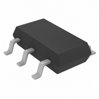
IC CONTROLLER HOT SWAP TSOT23-6
Manufacturer
Linear Technology
Type
Hot-Swap Controllerr
Datasheet
1.LTC4210-1CS6TRMPBF.pdf
(20 pages)
Specifications of LTC4210-1CS6#TR
Applications
General Purpose
Internal Switch(s)
No
Voltage - Supply
2.7 V ~ 16.5 V
Operating Temperature
0°C ~ 70°C
Mounting Type
Surface Mount
Package / Case
SOT-23-6 Thin, TSOT-23-6
Linear Misc Type
Positive Low Voltage
Family Name
LTC4210-1
Package Type
TSOT-23
Operating Supply Voltage (min)
2.7V
Operating Supply Voltage (max)
16.5V
Operating Temperature (min)
0C
Operating Temperature (max)
70C
Operating Temperature Classification
Commercial
Product Height (mm)
0.9mm
Product Length (mm)
2.9mm
Mounting
Surface Mount
Pin Count
6
Lead Free Status / RoHS Status
Contains lead / RoHS non-compliant
Lead Free Status / RoHS Status
Contains lead / RoHS non-compliant
Available stocks
Company
Part Number
Manufacturer
Quantity
Price
APPLICATIO S I FOR ATIO
A MOSFET with a V
meets the two criteria for all the LTC4210 applications
ranges from 2.7V to 16.5V. Typically most 10V gate rated
MOSFETs have V
greater, so no external V
are 4.5V gate rated MOSFETs with V
ratings of 20V.
In addition to the MOSFET gate drive rating and V
absolute maximum rating, other criteria such as V
I
operating area should also be carefully reviewed. V
should exceed the maximum supply voltage inclusive of
spikes and ringing. I
current limit, I
which together with V
At 2.7V supply voltage, the total of V
3.7% V
The maximum power dissipated in the MOSFET is
I
mum power dissipation, P
Given power dissipation, the MOSFET junction tempera-
ture, T
(T
The operating T
cation.
Next review the short-circuit condition under maximum
supply V
I
t
MOSFET. The operation during output short-circuit condi-
tions must be well within the manufacturer’s recom-
mended safe operating region with sufficient margin. To
ensure a reliable design, fault tests should be evaluated in
the laboratory.
V
Unlike most circuits, Hot Swap controllers typically are
not allowed the good engineering practice of supply
D(MAX)
LIMIT
LIMIT(MAX)
CBDELAY
IN
A
) and the MOSFET package thermal resistance (
TRANSIENT PROTECTION
2
J
, R
• R
OUT
can be computed from the operating temperature
IN(MAX)
with the maximum safe operating area of the
DS(ON)
DS(ON)
during the circuit breaker time-out interval of
error.
LIMIT
J
GS
, P
conditions and maximum current limit,
should be less than the T
and this should be less than the maxi-
. R
U
GS
absolute maximum ratings of 20V or
D
CB
,
D(MAX)
DS(ON)
absolute maximum rating of 20V
yields an error in the V
JA
GS
U
, T
Zener clamp is needed. There
determines the MOSFET V
D
should be greater than the
J(MAX)
allowed in that package.
W
GS
DS
and maximum safe
absolute maximum
+ V
CB
J(MAX)
of 0.1V yields
OUT
U
voltage.
specifi-
BDSS
BDSS
JA
GS
DS
).
,
bypass capacitors, since controlling the surge current to
bypass capacitors at plug-in is the primary motivation for
the Hot Swap controller. Although wire harness, back-
plane and PCB trace inductances are usually small, these
can create large spikes when large currents are suddenly
drawn, cut-off or limited. This can cause detrimental
damage to board components unless measures are taken.
Abrupt intervention can prevent subsequent damage
caused by a catastrophic fault but it does cause a large
supply transient. The energy stored in the lead/trace
inductance is easily controlled with snubbers and/or
transient voltage suppressors. Even when ferrite beads
are used for electromagnetic interference (EMI) control,
the low saturating current of ferrite will not pose a major
problem if the transient voltage suppressors with ad-
equate ratings are used. The transient associated with the
GATE turn off can be controlled with a snubber and/or
transient voltage suppressor. Snubbers such as RC net-
works are effective especially at low voltage supplies. The
choice of RC is usually determined experimentally. The
value of the snubber capacitor is usually chosen between
10 to 100 times the MOSFET C
snubber resistor is typically between 3 to 100 . When
the supply exceeds 7V or EMI beads exist in the wire
harness, a transient voltage suppressor and snubber are
recommended to clip off large spikes and reduce the
ringing. For supply voltages of 6V or below, a snubber
network should be sufficient to protect against transient
voltages. In many cases, a simple short-circuit test can be
performed to determine the need of the transient voltage
suppressor.
OVERVOLTAGE DETECTION USING THE TIMER PIN
Figure 11 shows a supply side overvoltage detection
circuit. A Zener diode, a diode and COMP2 threshold sets
the overvoltage threshold. Resistor R
diode voltage. Diode D1 blocks forward current in the
Zener during start-up or output short-circuit. R
C
TIMER
sets the overload noise filter.
LTC4210-1/LTC4210-2
OSS
. The value of the
B
biases the Zener
TIMER
17
421012f
with


