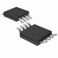
LTC4300A-1CMS8#TRPBF Linear Technology, LTC4300A-1CMS8#TRPBF Datasheet - Page 5

LTC4300A-1CMS8#TRPBF
Manufacturer Part Number
LTC4300A-1CMS8#TRPBF
Description
IC BUFFER BUS 2WR HOTSWAP 8-MSOP
Manufacturer
Linear Technology
Type
Hot-Swap Switchr
Datasheet
1.LTC4300A-1CMS8.pdf
(16 pages)
Specifications of LTC4300A-1CMS8#TRPBF
Applications
General Purpose, Buffer/Bus Extender
Internal Switch(s)
Yes
Voltage - Supply
2.7 V ~ 5.5 V
Operating Temperature
0°C ~ 70°C
Mounting Type
Surface Mount
Package / Case
8-TSSOP, 8-MSOP (0.118", 3.00mm Width)
Linear Misc Type
Positive Voltage
Package Type
MSOP
Operating Supply Voltage (min)
2.7V
Operating Supply Voltage (max)
5.5V
Operating Temperature (min)
0C
Operating Temperature (max)
70C
Operating Temperature Classification
Commercial
Product Depth (mm)
3mm
Product Height (mm)
0.86mm
Product Length (mm)
3mm
Mounting
Surface Mount
Pin Count
8
Lead Free Status / RoHS Status
Lead free / RoHS Compliant
Available stocks
Company
Part Number
Manufacturer
Quantity
Price
PI FU CTIO S
ENABLE/V
age. For the LTC4300A-1, this is a digital CMOS threshold
input pin. Grounding this pin puts the part in a low current
(<1 A) mode. It also disables the rise-time accelerators,
disables the bus precharge circuitry, drives READY low,
isolates SDAIN from SDAOUT and isolates SCLIN from
SCLOUT. Drive ENABLE all the way to V
operation. Connect ENABLE to V
being used. For the LTC4300A-2, this is the supply voltage
for the devices on the card I
resistors from SDAOUT and SCLOUT to this pin. Place a
bypass capacitor of at least 0.01 F close to this pin for best
results.
SCLOUT (Pin 2): Serial Clock Output. Connect this pin to
the SCL bus on the card.
SCLIN (Pin 3): Serial Clock Input. Connect this pin to the
SCL bus on the backplane.
GND (Pin 4): Ground. Connect this pin to a ground plane
for best results.
U
CC2
U
(Pin 1): Chip Enable Pin/Card Supply Volt-
U
2
C busses. Connect pull-up
CC
if this feature is not
CC
for normal
READY/ACC (Pin 5): Connection Flag/Rise-Time Accel-
erator Control. For the LTC4300A-1, this is an open-drain
NMOS output which pulls low when either ENABLE is low
or the start-up sequence described in the Operation sec-
tion has not been completed. READY goes high when
ENABLE is high and start-up is complete. Connect a 10k
resistor from this pin to V
LTC4300A-2, this is a CMOS threshold digital input pin
that enables and disables the rise-time accelerators on all
four SDA and SCL pins. Drive ACC all the way to the V
supply voltage to enable all four accelerators; drive ACC to
ground to turn them off.
SDAIN (Pin 6): Serial Data Input. Connect this pin to the
SDA bus on the backplane.
SDAOUT (Pin 7): Serial Data Output. Connect this pin to
the SDA bus on the card.
V
This is the supply voltage for the devices on the backplane
I
SCLIN (and also from SDAOUT and SCLOUT for the
LTC4300A-1) to this pin. Place a bypass capacitor of at
least 0.01 F close to this pin for best results.
2
CC
C busses. Connect pull-up resistors from SDAIN and
(Pin 8): Main Input Power Supply from Backplane.
LTC4300A-1/LTC4300A-2
CC
to provide the pull up. For the
sn4300a12 4300a12fs
5
CC2


