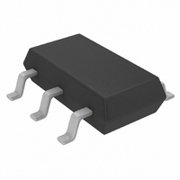
LTC4210-1IS6#TRM Linear Technology, LTC4210-1IS6#TRM Datasheet - Page 10

LTC4210-1IS6#TRM
Manufacturer Part Number
LTC4210-1IS6#TRM
Description
IC CONTROLLER HOT SWAP TSOT23-6
Manufacturer
Linear Technology
Type
Hot-Swap Controllerr
Datasheet
1.LTC4210-1CS6TRMPBF.pdf
(20 pages)
Specifications of LTC4210-1IS6#TRM
Applications
General Purpose
Internal Switch(s)
No
Voltage - Supply
2.7 V ~ 16.5 V
Operating Temperature
-40°C ~ 85°C
Mounting Type
Surface Mount
Package / Case
SOT-23-6 Thin, TSOT-23-6
Linear Misc Type
Positive Low Voltage
Family Name
LTC4210-1
Package Type
TSOT-23
Operating Supply Voltage (min)
2.7V
Operating Supply Voltage (max)
16.5V
Operating Temperature (min)
-40C
Operating Temperature (max)
85C
Operating Temperature Classification
Industrial
Product Height (mm)
0.9mm
Product Length (mm)
2.9mm
Mounting
Surface Mount
Pin Count
6
Lead Free Status / RoHS Status
Contains lead / RoHS non-compliant
Lead Free Status / RoHS Status
Contains lead / RoHS non-compliant
Other names
LTC4210-1IS6#TRMTR
Available stocks
Company
Part Number
Manufacturer
Quantity
Price
APPLICATIO S I FOR ATIO
LTC4210-1/LTC4210-2
If a 7m sense resistor with 1% tolerance is used for
current limiting, the nominal current limit is 7.14A. From
Equations 2 and 3, I
8.08A. For proper operation, the minimum current limit
must exceed the circuit maximum operating load current
with margin. The sense resistor power rating must exceed
V
Frequency Compensation
A compensation circuit should be connected to the GATE
pin for current limit loop stability.
Method 1
The simplest frequency compensation network consists
of R
Generally, the compensation value in Figure 2a is suffi-
cient for a pair of input wires less than a foot in length.
Applications with longer input wires may require the R
C
mance. For a pair of three foot input wires, users can start
with C
general rule for AC stability required is C
1k .
Method 2
The compensation network in Figure 2b is similar to the
circuitry used in method 1 but with an additional gate re-
sistor R
10
CB(MAX)
C
C
value to be increased for better fault transient perfor-
GATE
C
and C
C
G
= 47nF and R
. The R
2
= C
V
5V
/R
IN
C
SENSE(MIN)
ISS
(Figure 2a). The total GATE capacitance is:
V
G
Method 1
CC
+ C
LTC4210*
resistor helps to minimize high frequency
6
0.007
R
(2a)
SENSE
U
C
C
LIMIT(MIN)
SENSE
= 100 . Despite the wire length, the
GATE
.
5
U
Si4410DY
4
Q1
R
100
= 6.22A and I
C
C
10nF
C
+
W
C
L
**USE C
V
*ADDITIONAL DETAILS
OUT
OMITTED FOR CLARITY
OTHERWISE NOT REQUIRED
C
P
8nF and R
Figure 2. Frequency Compensation
LIMIT(MAX)
IF 0.2 F < C
U
L
C
< 9 F,
(4)
C
or
=
parasitic oscillations frequently associated with the power
MOSFET. In some applications, the user may find that R
helps in short-circuit transient recovery as well. However,
too large of an R
The recommended R
Usually, method 2 is preferred when the input supply volt-
age is greater than 10V. R
GATE pin’s internal zener clamp during transient events.
The recommended R
method 1. The parasitic compensation capacitor C
required when 0.2 F < load capacitance C
wise it is optional.
Parasitic MOSFET Oscillation
There are two possible parasitic oscillations when the
MOSFET operates as a source follower when ramping at
power-up or during current limiting. The first type of os-
cillation occurs at high frequencies, typically above 1MHz.
This high frequency oscillation is easily damped with R
mentioned in method 2.
The second type of oscillation occurs at frequencies be-
tween 200kHz and 800kHz due to the load capacitance
being between 0.2 F and 9 F, the presence of R
resistance, the absence of a drain bypass capacitor, a com-
bination of bus wiring inductance and bus supply output
impedance. There are several ways to prevent this second
type of oscillation. The simplest way is to avoid load ca-
pacitance below 10 F, the second choice is connecting an
external C
12V
V
IN
P
> 1.5nF.
V
Method 2
CC
LTC4210*
6
R
0.007
(2b)
SENSE
G
SENSE
value will slow down the turn-off time.
GATE
5
G
C
Si4410DY
range is between 5 and 500 .
4
and C
G
Q1
limits the current flow into the
R
200
R
100
4210 F02
G
C
C
10nF
C
C
values are the same as
C
2.2nF
P
**
+
L
C
L
< 9 F, other-
V
OUT
G
and R
421012f
P
G
as
is
G
C


