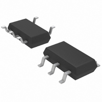
LTC4251-1IS6#TRPBF Linear Technology, LTC4251-1IS6#TRPBF Datasheet - Page 14

LTC4251-1IS6#TRPBF
Manufacturer Part Number
LTC4251-1IS6#TRPBF
Description
IC CTRLR HOTSWAP NEGVOLT SOT23-6
Manufacturer
Linear Technology
Type
Hot-Swap Controllerr
Datasheet
1.LTC4251CS6TRM.pdf
(24 pages)
Specifications of LTC4251-1IS6#TRPBF
Applications
General Purpose
Internal Switch(s)
No
Voltage - Supply
-36 V ~ -72 V
Operating Temperature
-40°C ~ 85°C
Mounting Type
Surface Mount
Package / Case
SOT-23-6 Thin, TSOT-23-6
Lead Free Status / RoHS Status
Lead free / RoHS Compliant
Available stocks
Company
Part Number
Manufacturer
Quantity
Price
APPLICATIONS INFORMATION
MOSFET selection is a three-step process. First, R
calculated, and then the time required to charge the load
capacitance is determined. This timing, along with the
maximum short-circuit current and maximum input volt-
age defines an operating point that is checked against the
MOSFET’s SOA curve.
To begin a design, first specify the required load current
and load capacitance, I
trip point (50mV/R
maximum load current. Note that maximum input current
to a DC/DC converter is expected at V
given by:
where 40mV represents the guaranteed minimum circuit
breaker threshold.
During the initial charging process, the LTC4251/
LTC4251-1/LTC4251-2 may operate the MOSFET in current
limit, forcing 80mV to 120mV across R
inrush current is given by:
Maximum short-circuit current limit is calculated using
maximum V
The TIMER capacitor C
slowest expected charging rate; otherwise TIMER might
time out before the load capacitor is fully charged. A value
for C
the load capacitor to charge. That time is given by:
LTC4251/LTC4251-1/
LTC4251-2
14
R
I
I
t
INRUSH(MIN)
SHORT-CIRCUIT(MAX)
CL CHARGE
S
T
=
is calculated based on the maximum time it takes
I
40mV
L(MAX)
SENSE
=
=
C • V
, or:
80mV
S
I
) should be set to accommodate the
R
S
L
=
and C
T
=
C
must be selected based on the
L
120mV
I
• V
INRUSH(MIN)
L
R
. The circuit breaker current
S
SUPPLY(MAX)
SUPPLY (MIN)
S
. The minimum
. R
(3)
(4)
(5)
(6)
S
S
is
is
Substituting Equation (4) for I
(6) with (2) gives:
Returning to Equation (2), the TIMER period is calcu-
lated and used in conjunction with V
I
tive MOSFET.
As a numerical design example, consider a 30W load,
which requires 1A input current at 36V. If V
72V and C
Equation (7) gives C
R
(4V), the calculated value should be multiplied by 1.5,
giving a nearest standard value of C
If a short-circuit occurs, a current of up to 120mV/40mΩ
= 3A will flow in the MOSFET for 5.7ms as dictated by
C
based on this criterion. The IRF530S can handle 100V and
3A for 10ms, and is safe to use in this application.
SUMMARY OF DESIGN FLOW
To summarize the design flow, consider the application
shown in Figure 2, which was designed for 50W:
Calculate maximum load current: 50W/36V = 1.4A; allow-
ing 83% converter efficiency, I
Calculate R
Calculate C
1.5X correction factor).
Calculate TIMER period: from Equation (2) the short-circuit
time-out period is t = 2.6ms.
Calculate maximum short-circuit current: from Equation
(5) maximum short-circuit current could be as high as
120mV/20mΩ = 6A.
Consult MOSFET SOA curves: the IRF530S can handle
6A at 72V for 5ms, so it is safe to use in this application.
SHORT-CIRCUIT(MAX)
T
SENSE
= 330nF in Equation (2). The MOSFET must be selected
C
T
=
, C
C
T
L
L
, TIMER current (230µA) and TIMER threshold
S
• V
T
= 100µF , Equation (3) gives R
: from Equation (3) R
: from Equation (7) C
SUPPLY (MAX)
(4V • 80mV)
to check the SOA curves of a prospec-
T
= 207nF . To account for errors in
• R
INRUSH(MIN)
IN (MAX)
S
• 230µA
S
T
= 20mΩ.
T
= 150nF (including
= 330nF .
= 1.7A.
SUPPLY(MAX)
SENSE
and equating
SUPPLY(MAX)
= 40mΩ;
(7)
425112fb
and
=


