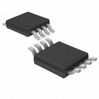
LTC4307CMS8#TRPBF Linear Technology, LTC4307CMS8#TRPBF Datasheet

LTC4307CMS8#TRPBF
Specifications of LTC4307CMS8#TRPBF
Available stocks
Related parts for LTC4307CMS8#TRPBF
LTC4307CMS8#TRPBF Summary of contents
Page 1
... SDAIN and SDAOUT, SCLIN and SCLOUT. READY is an open-drain output which indicates that the backplane and card sides are connected. , LT, LTC and LTM are registered trademarks of Linear Technology Corporation. All other trademarks are the property of their respective owners. Protected by U.S. Patents, including 7032051, 6356140, 6650174 2 ...
Page 2
LTC4307 ABSOLUTE AXI U RATI GND ................................................. – 0. SDAIN, SCLIN, SDAOUT, SCLOUT, READY, ENABLE .......................................... –0. Maximum Sink Current (SDAIN, SCLIN, SDAOUT, SCLOUT, READY) .............................................. 50mA Operating Temperature ...
Page 3
ELECTRICAL CHARACTERISTICS temperature range, otherwise specifi cations are at T SYMBOL PARAMETER Propagation Delay and Rise-Time Accelerators t SDA/SCL Propagation Delay High to Low PHL t SDA/SCL Propagation Delay Low to High PLH t SDA/SCL Transition Time Low to High ...
Page 4
LTC4307 TIMING DIAGRAMS ENABLE CONNECT READY Rising and Falling Propagation Delay and Rise and Fall Times for SDAIN, SDAOUT and SCLIN, SCLOUT SDAIN/SCLIN SDAOUT/SCLOUT 4 ENABLE, CONNECT, READY Timing t PLH_READY t t PLH_EN PHL_EN PLH PHL ...
Page 5
W U TYPICAL PERFOR A CE CHARACTERISTICS I vs Temperature CC 8 5.5V CC 8.0 7.7 7 3.3V CC 7.1 6 2.3V CC 6.5 6.2 5.9 –50 – 100 25 TEMPERATURE ...
Page 6
LTC4307 CTIO S ENABLE (Pin 1): Connection Enable Input. This is a 1.4V digital threshold input pin. For normal operation pull or tie ENABLE high. Driving ENABLE below 0.8V isolates SDAIN from SDAOUT, SCLIN from ...
Page 7
W BLOCK DIAGRA 8mA SDAIN 6 SLEW RATE DETECTOR 100k 100k 8mA SCLIN 3 SLEW RATE DETECTOR + – 0.55V CC + – 0.55V CC ENABLE + 1 – 1.4V OPERATION Start-Up When the LTC4307 fi rst receives power on ...
Page 8
LTC4307 OPERATION moment of connection, therefore minimizing the amount of disturbance caused by the I/O card. Once the LTC4307 comes out of UVLO, it monitors both the backplane and card sides for either a stop bit or bus idle condition ...
Page 9
OPERATION OUTPUT SIDE 50pF 1V/DIV 200ns/DIV Figure 2. Input-Output Rising Edge Waveforms Bus Stuck Low Timeout When SDAOUT or SCLOUT is low, an internal timer is started. The timer is only reset by that respective input going high ...
Page 10
... For a given I/O card, the LTC4307 drives the capacitance of everything on the card and the backplane must drive only the capacitance of the LTC4307, which is less than 10pF. Hot Swap is a trademark of Linear Technology Corporation. BACKPLANE ...
Page 11
APPLICATIONS INFORMATION The ENABLE pin is driven using a short pin. This is to ensure that a connection is not enabled until the transients associated with live insertion have settled. Figure 5 shows the LTC4307 in an application where all ...
Page 12
LTC4307 APPLICATIONS INFORMATION Systems with Supply Voltage Droop In large 2-wire systems, the V voltages seen by devices CC at various points in the system can differ by a few hundred 3. 10k 10k 10k SDA1 SCL1 ...
Page 13
TYPICAL APPLICATIONS TEMPERATURE SENSOR SHELF MANAGER DC/DC 3. 10k 10k V ENABLE SDAIN ShMC LTC4307 SCLIN High V Application 1.8k CC 1.8k R3 ENABLE 200Ω SCLIN SCLOUT R4 LTC4307 200Ω ...
Page 14
LTC4307 PACKAGE DESCRIPTION 3.5 ±0.05 1.65 ±0.05 2.15 ±0.05 (2 SIDES) 0.25 ± 0.05 0.50 BSC 2.38 ±0.05 (2 SIDES) RECOMMENDED SOLDER PAD PITCH AND DIMENSIONS NOTE: 1. DRAWING TO BE MADE A JEDEC PACKAGE OUTLINE M0-229 VARIATION OF (WEED-1) ...
Page 15
... LEAD COPLANARITY (BOTTOM OF LEADS AFTER FORMING) SHALL BE 0.102mm (.004") MAX Information furnished by Linear Technology Corporation is believed to be accurate and reliable. However, no responsibility is assumed for its use. Linear Technology Corporation makes no represen- tation that the interconnection of its circuits as described herein will not infringe on existing patent rights. ...
Page 16
... LTC4302-1/LTC4302-2 Addressable 2-Wire Bus Buffer LTC4303/LTC4304 Hot Swappable 2-Wire Bus Buffers with Stuck Bus Recovery LTC4305/LTC4306 2-/4-Channel, 2-Wire Bus Multiplexers with Capacitance Buffering ThinSOT is a trademark of Linear Technology Corporation Linear Technology Corporation 16 1630 McCarthy Blvd., Milpitas, CA 95035-7417 ● (408) 432-1900 FAX: (408) 434-0507 C2 0 ...


