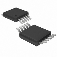
LTC4214-2CMS Linear Technology, LTC4214-2CMS Datasheet - Page 14

LTC4214-2CMS
Manufacturer Part Number
LTC4214-2CMS
Description
IC CTRLR HOTSWAP NEGVOLT 10MSOP
Manufacturer
Linear Technology
Type
Hot-Swap Controllerr
Datasheet
1.LTC4214-1CMS.pdf
(32 pages)
Specifications of LTC4214-2CMS
Applications
General Purpose
Internal Switch(s)
No
Voltage - Supply
6 V ~ 16 V
Operating Temperature
0°C ~ 70°C
Mounting Type
Surface Mount
Package / Case
10-TFSOP, 10-MSOP (0.118", 3.00mm Width)
Linear Misc Type
Negative Low Voltage
Family Name
LTC4214-2
Package Type
MSOP
Operating Supply Voltage (min)
-6V
Operating Supply Voltage (max)
-16V
Operating Temperature (min)
0C
Operating Temperature (max)
70C
Operating Temperature Classification
Commercial
Product Depth (mm)
3mm
Product Height (mm)
0.86mm
Product Length (mm)
3mm
Mounting
Surface Mount
Pin Count
10
Lead Free Status / RoHS Status
Contains lead / RoHS non-compliant
Lead Free Status / RoHS Status
Contains lead / RoHS non-compliant
Available stocks
Company
Part Number
Manufacturer
Quantity
Price
Company:
Part Number:
LTC4214-2CMS
Manufacturer:
LT
Quantity:
10 000
APPLICATIO S I FOR ATIO
LTC4214-1/LTC4214-2
UV/OV OPERATION
A low input to the UV comparator will reset the LTC4214
and pull the GATE and TIMER pins low. A low-to-high UV
transition will initiate an initial timing sequence if the other
interlock conditions are met. A high-to-low transition in
the UV comparator immediately shuts down the LTC4214,
pulls the MOSFET gate low and resets the latched PWRGD
high.
Overvoltage conditions detected by the OV comparator
will also pull GATE low, thereby shutting down the load.
However, it will not reset the circuit breaker TIMER,
PWRGD flag or shutdown cooling timer. Returning the
supply voltage to an acceptable range restarts the GATE
pin if all the interlock conditions except TIMER are met.
Only during the initial timing cycle does an OV condition
reset the TIMER.
DRAIN
Connecting an external resistor, R
DRAIN pin allows V
by large voltage transients. Below 3V, negligible pin leak-
age allows a DRAIN low comparator to detect V
than 1.232V (V
GATE low comparator, sets the PWRGD flag.
If V
4.2V and the current flowing in R
This current is scaled up 8 times during a circuit breaker
fault and is added to the nominal 40 A TIMER current. This
accelerates the fault TIMER pull-up when the MOSFET’s
drain-source voltage exceeds 4.2V and effectively short-
ens the MOSFET heating duration.
TIMER
The operation of the TIMER pin is somewhat complex as
it handles several key functions. A capacitor C
TIMER to provide timing for the LTC4214. Four different
charging and discharging modes are available at TIMER:
14
I
OUT
DRN
> V
DRNCL
V
OUT
DRNL
(4.2V), the DRAIN pin is clamped at about
R
D
V
OUT
U
DRNCL
). This condition, together with the
sensing without it being damaged
U
D
D
is given by:
W
, to the dual function
T
U
is used at
OUT
less
(1)
1) A 5 A slow charge; initial timing and shutdown cooling
delay.
2) A (40 A + 8 • I
3) A 5 A slow discharge; circuit breaker "cool off" and
shutdown cooling.
4) Low impedance switch; resets the TIMER capacitor
after an initial timing delay, in UVLO, in UV and in OV
during initial timing.
For initial start-up, the 5 A pull-up is used. The low
impedance switch is turned off and the 5 A current source
is enabled when the interlock conditions are met. C
charges to 3V in a time period given by:
When C
turns on and discharges C
and both SS and GATE are released.
CIRCUIT BREAKER TIMER OPERATION
If the SENSE pin detects more than a 50mV drop across
R
charges to 3V, the GATE pin pulls low and the LTC4214-1
latches off while the LTC4214-2 starts a shutdown cooling
cycle. The LTC4214-1 remains latched off until the UV pin
is momentarily pulsed low or TIMER is momentarily
discharged low by an external switch or V
UVLO and is then restored. The circuit breaker timeout
period is given by:
If V
pin leakage current, making I
V
the charging of C
Intermittent overloads may exceed the 50mV threshold at
SENSE, but, if their duration is sufficiently short, TIMER
will not reach 3V and the LTC4214 will not shut the external
OUT
S
, the TIMER pin charges C
t
t
OUT
> 4.2V (V
3
40
< 3V, an internal PMOS device isolates any DRAIN
T
V C
5
reaches 3V (V
•
3
A
A
V C
T
DRNCL
•
8
T
•
T
DRN
I
accelerates by 8 • I
DRN
) during the circuit breaker fault period,
) fast charge; circuit breaker delay.
TMRH
T
. A GATE start-up cycle begins
T
), the low impedance switch
DRN
with (40 A + 8 • I
= 0 A in Equation (3). If
DRN
of Equation (1).
IN
dips below
DRN
). If C
421412f
(2)
(3)
T
T


